


Section 24 A/D Converter
Page 1282 of 2108 R01UH0134EJ0400 Rev. 4.00
Sep 24, 2014
SH7262 Group, SH7264 Group
24.7 Usage Notes
When using the A/D converter, note the following points.
24.7.1 Module Standby Mode Setting
Operation of the A/D converter can be disabled or enabled using the standby control register. The
initial setting is for operation of the A/D converter to be halted. Register access is enabled by
clearing module standby mode. For details, see section 33, Power-Down Modes.
24.7.2 Setting Analog Input Voltage
Permanent damage to the LSI may result if the following voltage ranges are exceeded.
1. Analog input range
During A/D conversion, voltages on the analog input pins ANn should not go beyond the
following range: AVss ANn AVcc (n = 0 to 7).
2. AVcc and AVss input voltages
Input voltages AVcc and AVss should be PVcc 0.3 V AVcc PVcc and AVss = Vss. Do
not leave the AVcc and AVss pins open when the A/D converter is not in use and in software
standby mode. When not in use, connect AVcc to the power supply (PVcc) and AVss to the
ground (Vss).
3. Setting range of AVref input voltage
Set the reference voltage range of the AVref pin as 3.0 V AVref AVcc.
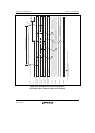
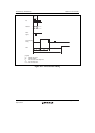
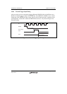
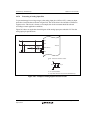
24.7.3 Notes on Board Design
In board design, digital circuitry and analog circuitry should be as mutually isolated as possible,
and layout in which digital circuit signal lines and analog circuit signal lines cross or are in close
proximity should be avoided as far as possible. Failure to do so may result in incorrect operation
of the analog circuitry due to inductance, adversely affecting A/D conversion values.
Digital circuitry must be isolated from the analog input signals (AN0 to AN3), analog reference
voltage (AVref), and analog power supply (AVcc) by the analog ground (AVss). Also, the analog
ground (AVss) should be connected at one point to a stable digital ground (Vss) on the board.