


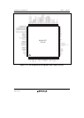
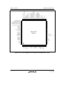
Section 1 Overview
R01UH0134EJ0400 Rev. 4.00 Page 21 of 2108
Sep 24, 2014
SH7262 Group, SH7264 Group
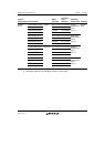
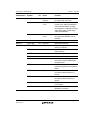
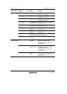
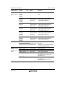
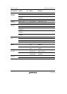
Classification Symbol I/O Name Function
Interrupts NMI I Non-maskable
interrupt
Non-maskable interrupt request pin.
Fix it high when not in use.
IRQ7 to IRQ0 I Interrupt requests
7 to 0
Maskable interrupt request pins.
Level-input or edge-input detection
can be selected. When the edge-
input detection is selected, the rising
edge, falling edge, or both edges
can also be selected.
PINT7 to PINT0 I Interrupt requests
7 to 0
Maskable interrupt request pins.
Only level-input detection can be
selected.
Address bus A25 to A0 O Address bus Outputs addresses.
Data bus D15 to D0 I/O Data bus Bidirectional data bus.
Bus control CS6 to CS0 O Chip select 6 to 0 Chip-select signals for external
memory or devices.
RD O Read Indicates that data is read from an
external device.
RD/WR O Read/write Read/write signal.
BS O Bus start Bus-cycle start signal.
AH O Address hold Address hold timing signal for the
device that uses the address/data-
multiplexed bus.
WAIT I Wait Inserts a wait cycle into the bus
cycles during access to the external
space.
WE0 O Byte select Indicates a write access to bits 7 to
0 of data of external memory or
device.
WE1 O Byte select Indicates a write access to bits 15 to
8 of data of external memory or
device.
DQML O Byte select Selects bits D7 to D0 when SDRAM
is connected.
DQMU O Byte select Selects bits D15 to D8 when
SDRAM is connected.