


R01UH0134EJ0400 Rev. 4.00 Page 2071 of 2108
Sep 24, 2014
Item Page Revision (See Manual for Details)
11.4.8 Complementary
PWM Mode
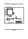
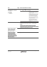
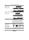
(1) Example of
Complementary PWM Mode
Setting Procedure
Figure 11.38 Example of
Complementary PWM Mode
Setting Procedure
542 Figure amended
[7] This setting is necessary only when no dead time should be
generated. Make appropriate settings in the timer dead time
enable register (TDER) so that no dead time is generated.
[8] Set the dead time in the dead time register (TDDR), 1/2 the
carrier cycle in the timer cycle data register (TCDR) and
timer cycle buffer register (TCBR), and 1/2 the carrier cycle
plus the dead time in TGRA_3 and TGRC_3. When no dead
time generation is selected, set 1 in TDDR and 1/2 the carrier
cycle + 1 in TGRA_3 and TGRC_3.
[8]
[9]
Dead time, carrier cycle
setting
PWM cycle output enabling,
PWM output level setting
Complementary PWM mode
setting
[10]
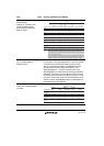
(2) Outline of
Complementary PWM Mode
Operation
(g) PWM Cycle Setting
550 Description amended
With dead time: TGRA_3 set value = TCDR set value + TDDR set value
TCDR set value > two times TDDR + 2
Without dead time: TGRA_3 set value = TCDR set value + 1
TCDR set value > 4
(j) Complementary PWM
Mode PWM Output
Generation Method
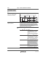
555 Description amended
A PWM waveform is generated by output of the output
level selected in the timer output control register in the
event of a compare-match between a counter and compare
register. While TCNTS is counting, compare register and
temporary register values are simultaneously compared to
create consecutive PWM pulses from 0 to 100%.
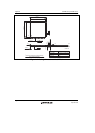
Figure 11.46 Example of
Complementary PWM Mode
Waveform Output (1)
556 Figure amended
T1 period
TGRA_3
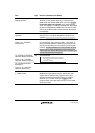
(k) Complementary PWM
Mode 0 and 100% Duty
Output
560 Description amended
100 duty output is performed when the compare register
value is set to H'0000. The waveform in this case has a
positive phase with a 100 on-state. 0 duty output is
performed when the compare register value is set to the
same value as TGRA_3.
(3) Interrupt Skipping in
Complementary PWM Mode
(c) Buffer Transfer Control
Linked with Interrupt
Skipping
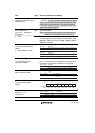
Figure 11.71 Example of
Operation when Buffer
Transfer is Linked with
Interrupt Skipping (BTE1 = 1
and BTE0 = 0)
576 Figure amended
2
2
01 10
TITCR[6:4]
TITCNT[6:4]