


iAPX 188 CPU
CPU
Internal Registers
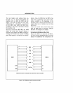
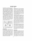
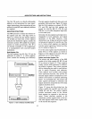
The added functionality
of
the iAPX
188
(i.e.,
timers, DMA, interrupt controller, and chip
selects) uses on-chip 16-bit control registers
for each integrated device. They are contained
in a 256-byte control block (see Figure
2)
in-
cluded in the
80188
CPU register architecture.
The control register block may be either
110
or
memory-mapped, based on initialization for a
new control block pointer in the
CPU. Except
for these additions, the register architecture
of
the iAPX
188
is
identical to the iAPX
88.
The
iAPX 188 is
similar
to
the
recently
announced iAPX
186.
The major difference
is
in the data bus width
(8
vs.
16
bits). Sixteen-bit
1-22
operands are fetched
or
written in two con-
secutive bus cycles. Both processors will ap-
pear identical to the software engineer, with
the exception
of
execution time. The internal
register structure
is
identical
and
all instruc-
tions have the same end result. The queue
length
is
shortened to four bytes rather than
six to prevent overuse
of
the
bus when pre-
fetching instructions.
To
further optimize the
queue, the
80188
will prefetch an instruction
each time there
is
a one-byte space available in
the queue, rather than waiting for a two-byte
space for a 16-bit instruction in the 80186. The
relationship between the
80188
and
80186
is
similar to the relationship between the
8088
and 8086.