


HARDWARE DESIGN
pIing capacitors are recommended to reduce
the noise on the power and ground lines.
TIMING
Pin
19
is
the clock input for basic timing of
the
8088. The maximum clock frequency
is
5
MHz
for the 8088, and 8
MHz
for the
8088-2. The clock signal
is
usually generated
by the 8284A (see pg. 3-13).
CONTROL STATUS
These lines specify the type of machine cycle
occurring and control external logic.
RD. The Read line
is
an active LOW output,
which indicates when the
CPU
is
reading
data
from a memory or
1/
a device.
This signal floats to 3-state
OFF
during "hold
acknowledge".
WR. The Write signal
is
an
active LOW out-
put, which indicates that the
CPU
is
output-
ting
data
onto the data bus to write it into a
memory
or
1/
a device.
This signal floats to 3-state
OFF
during "hold
acknowledge".
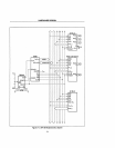
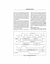
ALE. Address Latch Enable
is
an
output that
latches the addresses on the iAPX 88's address
bus. This signal is usually connected to the
STB input of
an
8282
latch, (Fig.
3-5).
The falling edge of ALE latches the address
on the system address bus to hold it through-
out the entire machine cycle, even though
some of the 8088's address pins will change
their functions during this time.
ALE
never
floats.
IO/M.
This output specifies whether the cur-
rent machine cycle will address
an
1/
a
or
a
memory device
(HIGH
=
I/O,
LOW =
Memory). This signal
is
valid during the entire
machine cycle, and floats to 3-state
OFF
dur-
ing
"hold acknowledge".
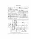
RESET. Providing
an
orderly way
to
start or
restart
an
iAPX
88
system, reset
is
an
active
HIGH
input to the 8088, synchronized by the
8284A.
3-3
Reset causes the processor to immediately
terminate its present activity and to condition
the bus as shown in Fig. 3-15. When reset
returns
LOW, the
8088
will begin executing
from memory location FFFF016.
During reset the processor
is
initialized to the
following conditions:
1)
The Flag register
is
reset
to
0000. This
disables interrupts and the single step mode.
2)
The DS, ES, SS and
IP
registers are reset
to
0000.
3)
The CS register
is
set to
FFFF
16.
Mo/
Mx. This input configures the
8088
in the
minimum mode when HIGH,
and
in the max-
imum mode when
LOW. This manual focuses
on minimum mode systems. Refer to pg. 3-24
for a discussion of maximum mode systems.
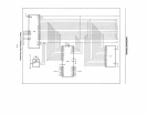
The pins
and
signals described above are suf-
ficient to completely control a small multi-
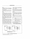
plexed bus system (Fig. 3-4). Larger systems,
however, use latches and transceivers for de-
multiplexing and increasing the drive of the
busses. Control signals for handling these
latches and for other functions are described
below as they are used in the
iAPX
88
larger
system (Fig. 3-5).
DT/it
Data
Transmit/ Receive
is
an
output,
controlling the direction in which the data
bus transceivers (8286s or 8287s) drive the
data on the
data
bus. When
HIGH,
data
is
transmitted onto the system
data
bus from
the
8088. When LOW,
data
is received from
the system bus to be read by the
8088. This
signal floats to 3-state
OFF
during "hold
acknowledge".
DEN. The
Data
Enable output drives the
output enable of the 8286/8287
data
bus
transceivers. This prevents bus contention by
disabling the data bus transceivers while the
8088
is
driving addresses on the address/
data
bus.