


iAPX 88/10
External Synchronization
via
TEST
As
an
alternative
to
interrupts, the 8088 provides a
single software-testable input pin
(TESn. This input is
utilized by executing a
WAIT instruction. The single
WAIT instruction is repeatedly executed until the
TEST
input goes active (LOW). The execution of WAIT does
not consume bus cycles once the queue is
full.
If
a local bus request occurs during WAIT execution, the
8088 3-states all output drivers.
If
interrupts are enabled,
the
8088 will recognize interrupts and process them.
The
WAIT instruction is then refetched, and reexecuted.
Basic System Timing
In minimum mode, the MN/MX pin is strapped to
Vee
and the processor
emits
bus control signals compatible
with the
8085 bus structure.
In
maximum mode, the
MN/MX pin is strapped to GND and the processor
emits
coded status information which the 8288 bus controller
uses to generate MULTIBUS compatible bus control
signals.
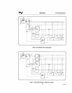
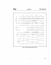
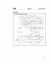
System Timing - Minimum System
(See
Figure
8,)
The
read
cycle begins in
T1
with the assertion of the
ad-
dress latch enable (ALE) signal. The trailing (low gOing)
edge
of
this signal is used to latch the address informa·
tion, which is valid
on
the address/data bus (ADO-AD7)
at this time, into the 8282/8283 latch. Address lines
A8
through A
15
do not need to
be
latched because they
re-
main valid throughout the bus cycle. From
T1
to
T4
the
10/M
signal indicates a memory
or
I/O
operation. At
T2
the address is removed from the address/data bus and
the bus goes to a high impedance state.
The~ad
con-
trol signal is also asserted at
T2.
The read
(RD)
signal
causes the addressed device
to
enable its data bus
drivers
to
the local bus. Some time later, valid data will
be
availabLe
on
the bus and the addressed device will
drive the READY line HIGH. When the processor returns
the read
Signal to a HIGH level, the addressed device
will again 3-state its bus drivers.
If a transceiver
(8286/8287) is required
to
buffer the 8088 local bus,
signals
DT/R
and
DEN
are provided
by
the
8088.
A write cycle also begins with the assertion of ALE and
the emission of the address. The
101M
Signal is again
asserted
to
indicate a memory or
110
write operation.
In
T2,
immediately following the address emission, the
processor
em
its the data to
be
written
into
the
ad-
dressed location. This data remains valid until at least
the middle
of
T4.
During
T2, T3,
and T
w
, the processor
asserts
tile
write control signal. The write
(WR)
signal
becomes active at the beginning of
T2,
as
opposed to
the read, which is delayed somewhat into
T2
to provide
time for the bus to float.
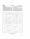
The basic dilference between the interrupt
acknowl-
edge cycle
Clnd
a read cycle is that the interrupt
acknowledge
(INTA) signal is asserted
in
place
of
the
read
(RD)
signal and the address bus is floated.
(See
Figure
9.l.ln
the second of two successive INTA cycles,
49
a byte
of
information is read from the data bus, as sup-
plied
by
the interrupt system logic (i.e. 8259A
priority
in-
terrupt controller). This byte identifies the source (type)
of
the interrupt. It is multiplied by four and used as a
pointer
into
the interrupt vector lookup table, as
.de-
scribed earlier.
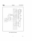
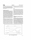
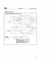
Bus
Timing - Medium Complexity Systems
(See
Figure 10J
For medium
complexity
systems, the M N/MX pin is con-
nected to GND and the 8288 bus controller is added
to
the system, as well
as
an
8282/8283 latch
for
latching
the system address, and
an
8286/8287 transceiver
to
allow for bus loading greater than the
8088
is capable
of
handling. Signals ALE, DEN, and
DT/R
are generated by
the 8288 instead of the processor in this configuration,
although
their
timing
remains relatively the same. The
8088 status outputs
(52,
S1,
and
SO)
provide type
of
cycle information and become 8288 inputs. This bus
cycle information specifies
read
(code, data,
or
110),
write (data
or
110),
interrupt acknowledge, or software
halt. The 8288 thus issues control
Signals specifying
memory read or write,
110
read
or
write, or interrupt
acknowledge. The 8288 provides two types
of
write
strobes, normal and advanced, to
be
applied
as
required.
The normal write strobes have data valid at the leading
edge of write. The advanced write strobes have the
same timing as read strobes, and hence, data is not
valid at the leading edge of write. The
8286/8287 trans-
ceiver receives the usual T and DE inputs from the
8288's
DT/R and
DEN
outputs.
The pOinter into the interrupt vector table, which is
passed during the second
INTA cycle, can derive from
an
8259A located
on
either the local bus
or
the system
bus.
If the master 8289A priority interrupt controller is
positioned
on
the local bus, a TTL gate is required
to
disable the 8286/8287 transceiver when reading from the
master 8259A during the interrupt acknowledge
se-
quence and software
"poll".
The 8088 Compared to the 8086
The 8088
CPU
is
an
8-bit processor designed around the
8086 internal structure. Most internal functions
of
the
8088 are identical
to
the equivalent
8086
functions. The
8088 handles the external bus the same way the 8086
does with the
distinction
of handling only 8
bits
at a
time.
Sixteen·bit operands are fetched or
written
in
two
consecutive bus cycles. Both processors will appear
identical
to
the software engineer,
with
the exception
of
execution time. The internal register structure is iden·
tical and all instructions have the same end result. The
differences between the
8088 and
8086
are outlined
below. The engineer who is unfamiliar with the
8086
is
referred to the iAPX
86,
88
User's Manual, Chapters 2 and
4,
for function description and instruction set information.
Internally, there are three differences between the 8088
and the 8086. All changes are related to the 8-bit bus in·
terface.
AFN-00826D