


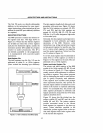
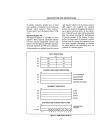

iAPX 188 CPU
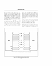
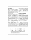
15 80188 REGISTER BLOCK 0
,-----------,
I
lAX
AH
AL
I
BX
BH
BL
I
I
I
CX
C
H
C
L
lOX
OH
DL
I
I
SP
I
I
BP
I
I
SI
I
I
01
I
I
IP
I
I
STATUS
I
I
CS
I
I
SS
I
I
OS
I
I
ES
I
L
_______
.-J
THE MEMORY
I RELOCATION REGISTER
OR I/O
MAPPED
15
DMACONTROL
CHIP SELECT
CONTROL
TIMER
CONTROL
INTERRUPT
CONTROL
1
B
256
YTES
J
Figure
2.
iAPX 188 Register Architecture
any external decode logic to select the re-
quired
I/O space
or
device. Each DMA chan-
nel
maintains
two
20-bit
source
and
destination pointers that can be incremented,
decremented,
or
left unchanged after each
transfer. Data transfers occur a byte at a time
and can be anywhere in the 1 megabyte
of
directly addressable memory space. This al-
lows a maximum transfer rate
of
1 megabyte
per second. The user can specify several differ-
ent modes
of
DMA operation via the on-chip
16-bit DMA channel control word.
By using the
80188
DMA facilities, data
Can
be
input onto local system memory, processed,
passed on to the host computer (if needed),
and output to another
I/O device, all by the use
of
the two independent, high-speed, on-chip
DMA channels.
Interrupt Controller
The
80188
interrupt
controller
resolves
priority among interrupt requests that arrive
simultaneously.
It
can accept interrupts from
up to five external hardware sources (NMI
+
4)
and internal sources as well (timers, DMA
channels). Each interrupt source has a pro-
grammable priority level and a preassigned
interrupt vector type, used to derive an ad-
dress to a table
in
memory where interrupt
1-21
service routine addresses are located. This en-
hancement
of
predefined vector types makes
the interrupt response time about
50% faster
than the typical iAPX
88
response time. The
8259A
programmable
interrupt
controller
(PIC) interrupt modes, such as fully nested
and specially fully nested, are provided by the
80188 as well. In addition, multiple 8259As can
be cascaded to provide the system with up to
128
external interrupts.
Chip Select/Ready Generation
The iAPX
188
contains programmable chip
select logic to provide chip select signals for
memory components, peripheral components,
and programmable ready (wait state) genera-
tion logic. The result
of
this integrated logic is a
lower system
part
count, since as many as
11
TTL
packs will be saved. In addition to a lower
system cost, the performance
of
the system
will improve as a result
of
the elimination
of
external propagation delays. Another advan-
tage
involves
flexibility in
the
choice
of
memory
component
size and speed.
Three
memory ranges (lower, middle, upper) can
be
programmed
to
variable
lengths
(IK,
2K,
4K,
...
256K) so that a variety
of
memory
chip sizes can be used. Further, anywhere
from zero to three wait states can be pro-
grammed so either high-speed
or
low-cost,
slower memories can be used. With respect to
the peripheral chip selects, as many as seven
different peripheral components can be ad-
dressed via
I/O
or
memory space. Again, pro-
grammable wait
states
may
be
injected
to
synchronize slower peripherals with the 80188
itself
or
memory.
The chip select/ready logic contributes to mak-
ing the iAPX
188
an optimum, low-cost choice
for a distributed processing node. In the past,
this necessary logic had to
be
designed, de-
bugged,
and
programmed.
Now,
with
the
80188, the design, debug, and programming
are done by initializing the associated 16-bit
on-chip control registers.