CHAPTER 4
APPLICATION EXAMPLES
INTRODUCTION
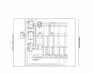
This chapter describes some iAPX
88
system
design examples, ranging from a simple
seven-chip system, to a larger system with
multiple
CPU's and coprocessors. The iAPX
nomenclature
is
used for configurations using
the
8088
or
8086
with
8089s
and
8087s.
MULTIPLEXED SYSTEM
The first iAPX
88
design example
is
a simple
multiplexed bus system, complete with
8088
CPU, 8284A clock generator, and - depend-
ing on the amount
of
memory and
I/O
desired -
2-5
multiplexed bus components.
This system demonstates the power, sim-
plicity, and density possible in iAPX
88
designs.
In its smallest configuration, this system
consists of only 4 chips:
CPU
Clock Generator
8088
8284A
8755A-2
8185
2K Bytes EPROM,
16
Lines
I/O
lK
Bytes
RAM
The configuration
we
will
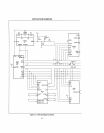
discuss has 7 chips:
8088
CPU
8284A Clock Generator
2 x 8755A-2 4K Bytes
EPROM,
32
I/O
Lines
2 x
8185
2K Bytes RAM
8155-2
256
Bytes
RAM,
22
I/O
Lines,
Timer/Counter
This system
is
built on a
95
mm X
105
mm
printed circuit board.
It
draws
400
-
600
mA
from a single
5V
power supply and includes
an
RS-232C interface,
an
LED for visual
communication, a RESET switch, and
JUMPER
options. A
sma:1l
monitor and
two programs - CHESS and TINY BASIC
-are
available
to
demonstrate
system
capabilities.
4-1
This system uses the 5MHz
8088
CPU. Its
memory and
I/O
components are connected
directly to the
8088's multiplexed address/
data bus, and no wait states are required.
Address Decoding
The memory and
I/O
address spaces are
decoded using upper address lines for linear
chip selects. Address lines AlO-A13 are
connected directly to the CS (chip select) and
CE (chip enable) inputs of the memory and
I/O
components. This eliminates the need for
special decoding
PROMs
or
TTL, re-
ducing component count and system com-
plexity.
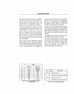
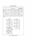
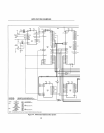
The address decoding table (Fig.
4-1)
lists
address line usage for memory and
I/O
address decoding.
CAUTION:
For
most systems using linear
chip selects, some addresses enable more than
one memory or
I/O
device at the same time.
For
instance, the 8755A-2 in location
E3
is
enables any time
All
is
HIGH. Another
device, the
8185
at
E6
is
enabled, when
Al3
is
LOW and
AW
is
HIGH. Although the
8755A-2
is
uniquely selected by address
locations F800H-FFFFH and the
8185
is
uniquely selected by 14H-17FFH, both com-
ponents are enabled by memory addresses
from
COOH to
FFFH.
Therefore, the pro-
grammer must NOT
use
this range of
addresses.
1/0
This system provides
54
I/O
lines, some
dedicated to the RS232C interface, the LED
output, and the
8155's
timer/counter. The
other
I/O
lines are available for general
purpose 1/
O.
The two
8755As
provide
321/0
lines, individually programmable as inputs
or
outputs. Three
of
these lines, P A
7,
PBO
and
PB7
of
E3,
implement the RS232C REC-
EIVE-DATA and TRANSMIT-DATA fun-
ctions, and the LED output.
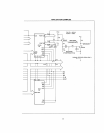
The implementation of the RS232C
interface
will be explained for a
few
interesting tricks


