


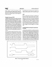
iAPX
8.8110
"wait"
states
(Tw)
are inserted between
T3
and T4. Each
inserted
"wait"
state is
of
the same duration
as
a
ClK
cycle. Periods can
occur
between 8088 driven bus cycles.
These are referred
to
as
"idle"
states (Ti),
or
inactive
ClK
cycles. The
processor
uses
these
cycles
for
internal
housekeeping.
During
T1
of
any bus cycle, the ALE (address latch enable)
signal
is emitted (by either the processor
or
the 8288 bus
controller, depending on the MN/MX strap). At
the
trailing
edge
of
this pulse, a valid address and certain status
information
for
the cycle may be latched.
Status bits
SO,
51,
and
S2
are used by the bus controller, in
maximum mode,
to
identify the type
of
bus transaction
according
to
the following table:
- - -
52
51
50
CHARACTERISTICS
a
(LOW)
0
0
Interrupt Acknowledge
a
0 1
Read
110
0
1
0
Write
1/0
a
1 1
Halt
1
(HIGH)
a 0
Instruction Fetch
1
0 1
Read
Data
from Memory
1
1
a
Write
Data
to
Memory
1
1 1
Passive
(no
bus
cycle)
Status bits
S3
through
S6
are multiplexed with high order
address bits and are therefore
valid
during
T2
through
T4.
S3
and
S4
indicate which segment register was used
for
this bus cycle
in
forming
the address according
to
the
following table:
54 53
CHARACTERISTICS
a
(LOW)
a Alternate
Data
(extra segment)
0
1
Stack
1
(HIGH)
0
Code
or
None
1
1
Data
S5
is a reflection
of
the PSW
interrupt
enable bit.
S6
is
always equal
to
O.
I/O Addressing
In the 8088, I/O operations can address up
to
a
maximum
of
64K I/O registers. The
I/O
address appears in the same
format
as
the memory address on bus lines A15-AO. The
address lines A19-A16 are zero in I/O operations. The vari-
able I/O instructions, which use register
DX
as
a pointer,
have
full address capability, while tne
direct
I/O instruc-
tions
directly
address one
or
two
of
the
256
I/O·byte
locations in page 0
of
the I/O address space. I/O
ports
are
addressed in the same manner
as
memory locations.
Designers familiar
with
the 8085
or
upgrading
an 8085
design
should
note
that
the 8085 addresses
I/O
with
an
8-bit address on both
halves of the 16-bit address bus. The
8088 uses a full 16-bit address on its lower 16 address
lines.
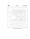
47
EXTERNAL
INTERFACE
Processor Reset
.and
Initialization
Processor initialization
or
start up is accomplished
with
activation (HIGH)
of
the RESET pin. The 8088 RESET is
required to be
HIGH for greater than
four
clock
cycles. The
8088 will terminate operations on the high-going edge
of
RESET and will remain
dormant
as
long
as
RESET is HIGH.
The low-going transition
of
RESET triggers an internal
reset sequence for approximately 7 clock cycles.
After
this
interval the 8088 operates normally, begiA-ning witt! ~e
instruction in absolute location
FFFFOH.
(See Figure 4.)
The
RESET
input
is internally synchronized
to
the proces-
sor
clock. At initialization, the HIGH
to
LOW
transition
of
RESET must
occur
no
sooner than 50
J-LS
after
power
up, to
allow complete initialization
of
the 8088.
If INTR
is asserted
sooner
than nine clock cycles
after
the
end
of
RESET,
the processor may execute
one
instruction
before responding to the interrupt.
All 3-state
outputs
float to 3-state OFF
during
RESET.
Status is active in the
idle state
for
the
first
clock
after
RESET becomes active and then floats
to
3-state
OFF.
Interrupt Operations
Interrupt
operations fall into two classes:
software
or
hardware initiated. The software initiated
interrupts
and
software aspects
of
hardware interrupts are specified
in
the instruction set
description
in the iAPX 88
book
or
the
iAPX 86,88 User's
Manual. Hardware interrupts can be
classified
as
nonmaskable
or
maskable.
Interrupts
result in a transfer
of
control to a new
program
location. A 256 element table
containing
address
pointers
to
the
interrupt
service program locations resides in abso-
lute locations 0
through
3FFH (see Figure 4),
which
are
reserved
for
this purpose. Each element
in
the table is 4
bytes in size and corresponds
to
an interrupt
"type."
An
interrupting
device supplies
an
8-bit type number,
during
the
interrupt
acknowledge sequence, which is used to
vector
through
the
appropriate
element to
the
new inter-
rupt service program location.
Non-Maskable Interrupt (NMI)
The processor provides a single non-maskable
interrupt
(NMI) pin which has
higher
priority
than the maskable
interrupt
request (INTR) pin. A typical use
would
be
to
activate a power failure routine. The NMI is
edge-triggered
on a
lOW
to
HIGH transition. The activation
of
this pin
causes a type 2 interrupt.
NMI is required to have a duration in the HIGH state
of
greater than
two
clock
cycles,
but
is
not
required
to
be
synchronized
to
the clock. Any higher going
transition
of
NMI is latched on-Chip and will be serviced at
the
end
of
the current
instruction
or
between
whole
moves
(2
bytes in
the case
of
word moves)
of
a
block
type instruction. Worst
case response
to
NMI
would
be
for multiply, divide, and
variable shift instructions. There is
no
specification on
the
occurrence
of
the
low-going
edge;
it
may
occur
AFN-OOB260