


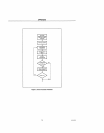
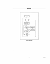
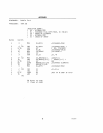
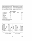
APPENDIX
The topics discussed are Architecture, Memory Timing,
Instruction Sets, and Addressing Modes. For more
com-
plete descriptions, refer to Intel's
8086
Family Users'
Manual and Motorola's MC6809 Preliminary Program-
ming
Manual or other related literature.
iAPX 88
The Intel
8088
(or 88/10)
is
the host processor
of
the
iAPX
88
microcomputer system. The 88/10
is
an
N-channel
MaS
microprocessor
which,
currently has a
maximum clock rate
of
5 MHz. Internallylhe
88110
is
a
microcoded 16-bit processor which multiplexes a 16-bit
internal data bus onto an 8-bit system data bus for
ex-
ternal communication. The address space
is
one mega-
byte which
is
segmented to support modular programm-
ing.
Except for the implementation
of
the
Bus
Interface
Unit the 88/10
is
identical to the Intel 86/10
microprocessor.
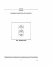
The
architecture
of
the 88/10
is
divided into two
separate processing units, the
Bus
Interface Unit (BIU)
and the Execution Unit (EU). These two units perform
separate functions in parallel to maximize throughput.
The
EU
contains the 16-bit arithmetic/logic unit (ALU)
as
well
as
the general registers and flags
of
the CPU. It
is
responsible for executing instructions, and communi-
cates only with the BIU. The BIU performs all bus .
operations needed by the
EU.
It
contains the segment
registers, the instruction pointer, the bus control logic
and the instruction queue. Because the
BIU operates in
parallel with the
EU, instruction fetches overlap instruc-
tion execution. The result
is
efficient utilization
of
the
system
bus and transparent instruction prefetch.
The
88/10 contains three sets
of
four 16-bit registers,
and nine one-bit flags. The four data group registers,
AX,
BX, CX and DX,
as
well
as the four pointer and in-
dex
registers, SP, BP, SI and DI, are all 16-bits wide and
can be used as source
anq destination in most arithmetic
and logic operations. All eight
of
these general registers
function as accumulators for many instructions. The
data group registers, AX, BX,
CX and DX can also be
used as eight 8-bit accumulators for byte operations.
The pointer and index registers also serve
as
address
registers in addition to their
genera,!
register functions.
The SI and DI registers function as the source and
destination pointers for the string operations. The Stack
Pointer register (SP)
is
used in stack operations,
and
the
BP
register
is
a base pointer for stack relative Based Ad-
.
dressing modes frequently used in high level language
programming. The four 16-bit segment registers, CS,
DS,
SS
and ES, provide memory segmentation expand-
ing
the address space to one megabyte.
The iAPX
88
uses a four-clock basic bus cycle. The nor-
mal memory access time
is
460 nsec. To use memories
slower than this, wait states
of
ZOO
nsec can be added.
Using one wait state produces a memory access time
of
660
nsec.
22
The iAPX 88/10 instruction set operates on bits,
BCD.
digits, ASCII digits, 8-bit bytes, 16-bit words, and
signed or unsigned integers. Many
of
the two operand
instructions allow both operands to reside in registers,
or one in a register and one in memory. The order of the
operands
is
interchangeable, and the location
of
either
source operand may serve
as
the destination for the
result. The arithmetic instructions include
8-
or 16-bit
Add, Subtract, Multiply, Divide and Compare
of
signed
or unsigned integer values. The iAPX
88
instructions
!lre identical
to
those
of
the iAPX
86
providing complete
software compatibility.
Twenty-four addressing modes are available to directly
or indirectly access data and operands. These modes
allow from one to four component addressing using
combinations
of
segment, base, and index registers,
and/or
8-
or f6-bit displacements. The string instruc-
tions provide auto increment and auto decrement
ad-
dressing, memory to memory operations, and have an
optional repeat prefix.
The iAPX
88
in the minimum mode supports the
hold/
hold acknowledge protocol to enable bus control to be
transferred to another bus master such
as
a DMA con-
troller.
It
can also be configured in the maximum mode
with two request/grant lines, each
of
which can support
multiple bus masters for coprocessor designs using the
8087
Numeric Data Processor
and/or
the
8089
110
Processor (iAPX 88/20, iAPX 88/21, iAPX 88/11).
Even though not considered on these benchmarks, the
8087
(iAPX 88/20) uniquely enhances the iAPX 88/10
(86/10) capabilities with
68
additional instructions, in-
cluding 64-bit floating point and transcendental func-
tions, eight 80-bit stack oriented registers and seven ad-
ditional·numeric data types.
The iAPX
88
provides nonmaskable software (internal)
interrupts and maskable or nonmaskable.hardware
(ex-
ternal) interrupts. The interrupt structure supports up to
256
different interrupt types using an interrupt vector
table located in memory. For more information regard-
ing interrupts
see
your local Intel office.
MC6809
The Motorola MC6809
is
an N-channel random logic
MaS
microprocessor which
is
available at 1.0 MHz,
1.5
MHz or 2.0 MHz clock rates. The MC6809 can address
up to
64
kbytes
of
memory. The A and B registers are
two 8-bit accumulators which
may be concatenated into
a single 16-bit accumulator, the D register. There are
four pointer registers: X,
Y,
U and
S.
All are 16-bits
wide and function primarily as base registers for
memory addressing. The
U and S registers are also used
for manipulating the hardware and user stacks. The
16-bit program counter (PC) points
to
the address
of
the
next instruction, and can. also
be
operated on for control
transfer. The 8-bit Direct Page Register (DPR)
is
used to
contain the upper eight address bits for some addressing
AFN 01532A