


HARDWARE DESIGN
Conveniently, most. Intel peripherals,
EPROMs and RAMs in the iAPX
88
family
provide output enable
or
read inputs which
prevent this from happening.
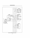
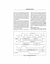
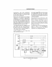
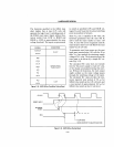
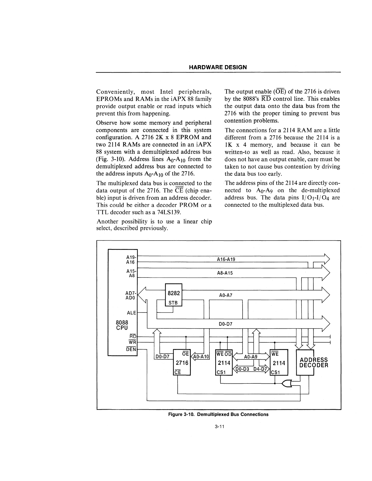
Observe how some memory and peripheral
components are connected in this system
configuration. A 2716 2K x 8
EPROM
and
two 2114 RAMs are connected in
an
iAPX
88
system with a demultiplexed address bus
(Fig. 3-10). Address lines Ao-A
10
from the
demultiplexed address bus are connected to
the address inputs
Ao-AlO
of the 2716.
The multiplexed data bus
is
connected to the
data output of the
2716.
The CE (chip ena-
ble) input
is
driven from an address decoder.
This could be either a decoder
PROM
or a
TIL
decoder such as a 74LS139.
Another possibility
is
to use a linear chip
select, described previously.
A19-
A16
A15-
AS
k:
ro-
AD7-
8282
ADD
,-
STB
ALE
-
~
8088
CPU
RD
-
WR
-
r
~Atui
DEN
-
00-'57
OE
AO-A10
2716~
CL-
The output enable (OE) of the
2716
is
driven
by the
8088's
RD
control line. This enables
the output data onto the data bus from the
2716
with the proper timing
to
prevent bus
contention problems.
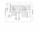
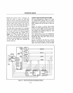
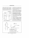
The connections for a
2114
RAM are a little
different from a
2716
because the
2114
is
a
lK
x 4 memory, and because it can be
written-to as
well
as read. Also, because it
does not have
an
output enable, care must be
taken to not cause bus contention by driving
the data bus too early .
. The address pins of the 2114 are directly con-
nected to
AO-A9
on the de-multiplexed
address bus. The data pins
1/01-1/04
are
connected to the multiplexed data bus.
A16-A19
~
AS-A15
AD-A7
00-07
r-
r-
;==!
T
r-
I-
,llr
I
ADD~ESS
WEOD
AO-A9
WE
2114
04~
2114
DECyDER
T-
00-03
CS1
l~
I
Figure 3-10. Oemultiplexed Bus Connections
3-11