Section 9 Bus State Controller
R01UH0134EJ0400 Rev. 4.00 Page 351 of 2108
Sep 24, 2014
SH7262 Group, SH7264 Group
Tpcm1w
CKIO
A25 to A0
CExx
RD/WR
RD
D15 to D0
WE
D15 to D0
BS
Read
Write
Tpcm2Tpcm0 Tpcm1 Tpcm1wTpcm0w Tpcm2wTpcm1w Tpcm1w
WAIT
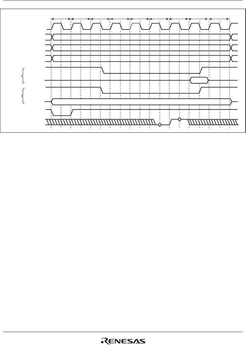
Figure 9.40 Wait Timing for PCMCIA Memory Card Interface
(TED[3:0] = B'0010, PCW[3:0] = B'0000, TEH[3:0] = B'0001, Hardware Wait = 1)
A port is used to generate the REG signal that switches between the common memory and
attribute memory. As shown in the example in figure 9.41, when the total memory space necessary
for the common memory and attribute memory is 32 Mbytes or less, pin A24 can be used as the
REG signal to allocate a 16-Mbyte common memory space and a 16-Mbyte attribute memory
space.


