Section 20 Controller Area Network
Page 1014 of 2108 R01UH0134EJ0400 Rev. 4.00
Sep 24, 2014
SH7262 Group, SH7264 Group
BCR0 (Address = H'006)
1514131211109876543210
0000000000000000
RRRRRRRRR/W R/W R/W R/W R/W R/W R/W R/W
BRP[7:0]
Bit:
Initial value:
R/W:
--------
Bits 8 to 15: Reserved. The written value should always be '0' and the returned value is '0'.
Bits 7 to 0—Baud Rate Pre-scale (BRP[7:0] = BCR0 [7:0]): These bits are used to define the
peripheral clock periods contained in a Time Quantum.
Bit 7:
BRP[7]
Bit 6:
BRP[6]
Bit 5:
BRP[5]
Bit 4:
BRP[4]
Bit 3:
BRP[3]
Bit 2:
BRP[2]
Bit 1:
BRP[1]
Bit 0:
BRP[0]
Description
0 0 0 0 0 0 0 0 2 X peripheral clock
(Initial value)
0 0 0 0 0 0 0 1 4 X peripheral clock
0 0 0 0 0 0 1 0 6 X peripheral clock
:
:
:
:
:
:
:
:
:
:
:
:
:
:
:
:
2*(register value + 1) X
peripheral clock
1 1 1 1 1 1 1 1 512 X peripheral clock
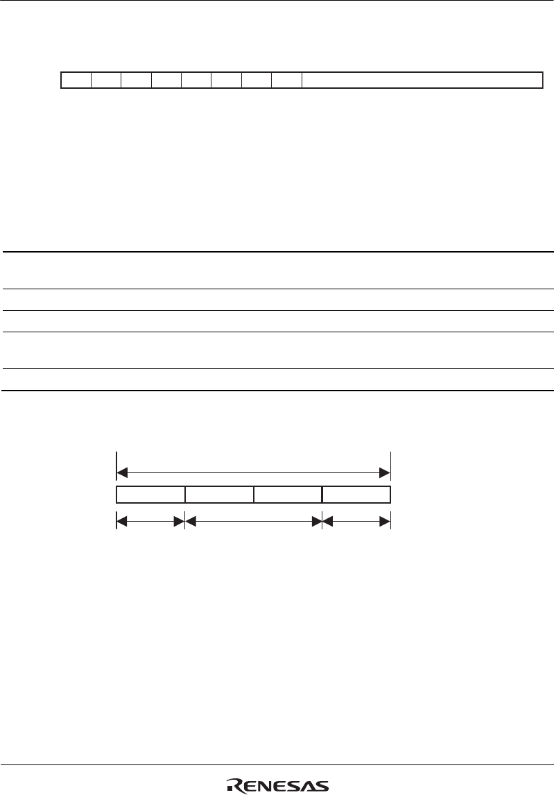
Requirements of Bit Configuration Register
SYNC_SEG PRSEG PHSEG1
TSEG1
1-bit time (8-25 quanta)
1 4-16 2-8
TSEG2
Quantum
PHSEG2
SYNC_SEG: Segment for establishing synchronisation of nodes on the CAN bus. (Normal bit
edge transitions occur in this segment.)
PRSEG: Segment for compensating for physical delay between networks.
PHSEG1: Buffer segment for correcting phase drift (positive). (This segment is extended
when synchronisation (resynchronisation) is established.)
PHSEG2: Buffer segment for correcting phase drift (negative). (This segment is shortened
when synchronisation (resynchronisation) is established)
TSEG1: TSG1 + 1


