Section 4 Boot Mode
R01UH0134EJ0400 Rev. 4.00 Page 111 of 2108
Sep 24, 2014
SH7262 Group, SH7264 Group
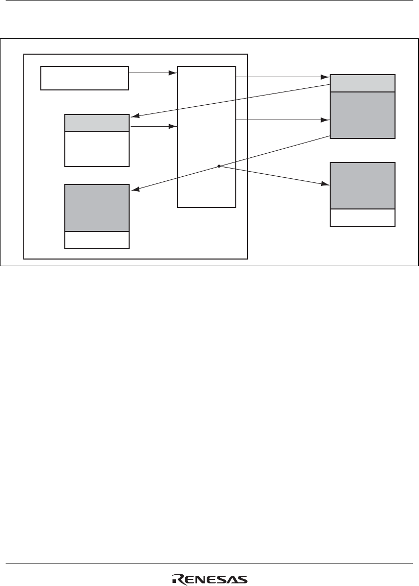
Figure 4.1 is a schematic view of the specification for boot modes 1 and 3.
On-chip ROM for boot
initiation (not publicly disclosed)
Loader program
(8 KB)
Loader program
(8 KB)
High-speed on-chip RAM
On-chip RAM
Application
program
External RAM
Serial flash memory
Application
program
Application
program
Renesas serial
peripheral
interface
Channel 0
H'FFF8 0000
H'FFF8 1FFF
Read request
Read
Read
Read request
This LSI
(1) Program execution
(2) Loading into high-speed
on-chip RAM
(3) Loading into external
or on-chip RAM
Figure 4.1 Schematic View of Specification for Boot Modes 1 and 3
4.3.3 Boot Mode 2
In boot mode 2, booting up is from NAND flash memory, which is connected to the NAND flash
memory controller. Suitable NAND flash memory has a large block size (2048 64) and takes
five-byte addresses (has a capacity of 2 GB or greater). Furthermore, errors in up to four locations
are correctable. The flow of initiation for a NAND-flash boot is as described below.
(1) Execution from on-Chip ROM of the Program for Boot Initiation
After release from the power-on reset state, the CPU executes the boot initiation program that has
been stored in on-chip ROM (and is not publicly disclosed).
(2) Transfer of the Loader Program
Starting with transfer from the respective first locations, the 8-KB loader program is transferred
from NAND flash memory, which is connected to the NAND flash memory controller, to high-
speed on-chip RAM. Transfer and checking by the loader program proceed as follows.


