


Section 1 Overview
R01UH0134EJ0400 Rev. 4.00 Page 27 of 2108
Sep 24, 2014
SH7262 Group, SH7264 Group
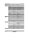
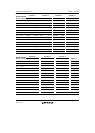
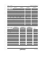
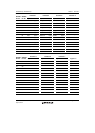
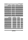
Classification Symbol I/O Name Function
Video display
controller 3
LCD_DATA15 to
LCD_DATA0
O Output data Data output pin for panel.
LCD_DE O Data enable Data enable output pin for panel.
LCD_VSYNC O VSYNC output VSYNC output pin for panel.
LCD_HSYNC O HSYNC output HSYNC output pin for panel.
LCD_CLK O Panel clock Panel clock output pin.
LCD_EXTCLK I Panel clock
source
Panel clock source input pin.
LCD_M_DISP O LCD current
alternation
LCD current alternating signal pin.
DV_DATA7 to
DV_DATA0
I Input data Data input pin for BT.601 and
BT.656.
DV_VSYNC I VSYNC input VSYNC input pin.
DV_HSYNC I HSYNC input HSYNC input pin.
DV_CLK I Input clock Clock input signal pin for BT.601 and
BT.656.
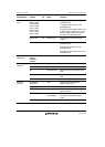
SD host
interface
SD_CLK O SD clock Output pin for SD clock.
SD_CMD I/O SD command SD command output and response
input signal.
SD_D3 to
SD_D0
I/O SD data SD data bus signal.
SD_CD I SD card detection SD card detection.
SD_WP I SD write
protection
SD write protection signal.
A/D converter AN7 to AN0 I Analog input pins Analog input pins.
Only AN3 to AN0 can be used in the
SH7262 Group.
ADTRG I A/D conversion
trigger input
External trigger input pin for starting
A/D conversion.
AVcc I Analog power
supply
Power supply pin for A/D converter.
AVss I Analog ground Ground pin for A/D converter.
AVref I Analog reference
voltage
Reference voltage pin for A/D
converter.