Section 11 Multi-Function Timer Pulse Unit 2
R01UH0134EJ0400 Rev. 4.00 Page 495 of 2108
Sep 24, 2014
SH7262 Group, SH7264 Group
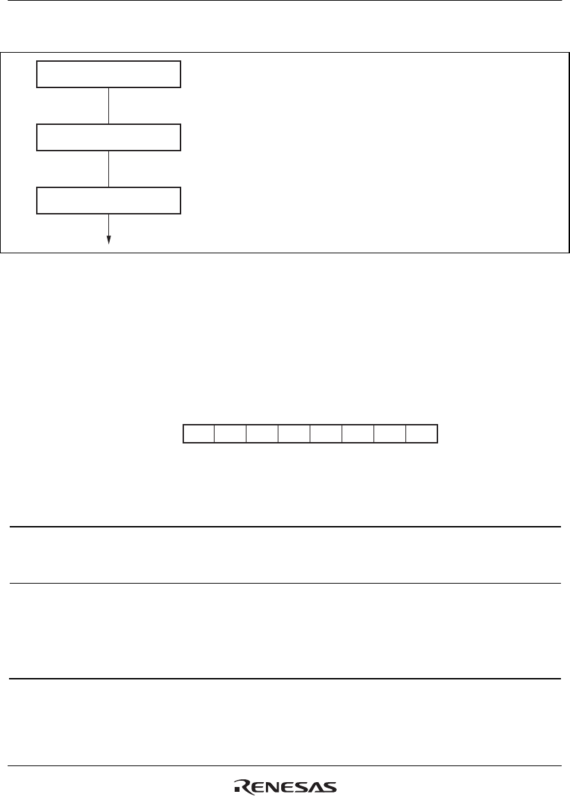
Figure 11.3 shows an example of the PWM output level setting procedure in buffer operation.
Set bit TOCS
Set TOCR2
Set TOLBR
[1]
[2]
[3]
[1] Set bit TOCS in TOCR1 to 1 to enable the TOCR2 setting.
[2] Use bits BF1 and BF0 in TOCR2 to select the TOLBR buffer
transfer timing. Use bits OLS3N to OLS1N and OLS3P to OLS1P
to specify the PWM output levels.
[3] The TOLBR initial setting must be the same value as specified in
bits OLS3N to OLS1N and OLS3P to OLS1P in TOCR2.
Figure 11.3 PWM Output Level Setting Procedure in Buffer Operation
11.3.20 Timer Gate Control Register (TGCR)
TGCR is an 8-bit readable/writable register that controls the waveform output necessary for
brushless DC motor control in reset-synchronized PWM mode/complementary PWM mode. These
register settings are ineffective for anything other than complementary PWM mode/reset-
synchronized PWM mode.
Bit:
Initial value:
R/W:
7654321
0
10000000
R R/W R/W R/W R/W R/W R/W R/W
- BDC N P FB WF VF UF
Bit Bit Name
Initial
value R/W Description
7 1 R Reserved
This bit is always read as 1. The write value should
always be 1.
6 BDC 0 R/W Brushless DC Motor
This bit selects whether to make the functions of this
register (TGCR) effective or ineffective.
0: Ordinary output
1: Functions of this register are made effective


