


Section 11 Multi-Function Timer Pulse Unit 2
Page 492 of 2108 R01UH0134EJ0400 Rev. 4.00
Sep 24, 2014
SH7262 Group, SH7264 Group
Bit Bit Name
Initial
value R/W Description
0 OLS1P 0 R/W Output Level Select 1P*
This bit selects the output level on TIOC3B in reset-
synchronized PWM mode/complementary PWM mode.
See table 11.36.
Note: * Setting the TOCS bit in TOCR1 to 1 makes this bit setting valid. If there is no dead time,
the reverse phase output is the inversion of the forward phase. Set OLSiP and OLSiN
to the same value (i = 1, 2, or 3).
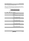
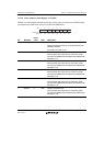
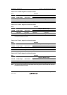
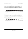
Table 11.30 Setting of Bits BF1 and BF0
Bit 7 Bit 6 Description
BF1 BF0 Complementary PWM Mode Reset-Synchronized PWM Mode
0 0 Does not transfer data from the
buffer register (TOLBR) to TOCR2.
Does not transfer data from the
buffer register (TOLBR) to TOCR2.
0 1 Transfers data from the buffer
register (TOLBR) to TOCR2 at the
crest of the TCNT_4 count.
Transfers data from the buffer
register (TOLBR) to TOCR2 when
TCNT_3/TCNT_4 is cleared
1 0 Transfers data from the buffer
register (TOLBR) to TOCR2 at the
trough of the TCNT_4 count.
Setting prohibited
1 1 Transfers data from the buffer
register (TOLBR) to TOCR2 at the
crest and trough of the TCNT_4
count.
Setting prohibited
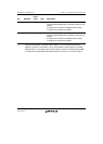
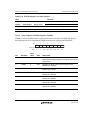
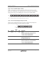
Table 11.31 TIOC4D Output Level Select Function
Bit 5 Function
OLS3N Initial Output Active Level
Compare Match Output
Up Count Down Count
0 High level Low level High level Low level
1 Low level High level Low level High level
Note: The reverse phase waveform initial output value changes to the active level after elapse of
the dead time after count start.