


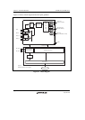


Section 5 Clock Pulse Generator
R01UH0134EJ0400 Rev. 4.00 Page 123 of 2108
Sep 24, 2014
SH7262 Group, SH7264 Group
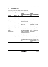
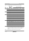
Bit Bit Name
Initial
Value R/W Description
14 CKOEN2 0 R/W Clock Output Enable 2
Specifies whether the CKIO pin outputs clock signals
or is fixed to the low level when the gain of the crystal
oscillator for the XTAL pin is changed.
If this bit is set to 1, the CKIO pin is fixed to the low
level when the gain of the crystal oscillator for the
XTAL pin is changed. Therefore, the malfunction of an
external circuit caused by an unstable CKIO clock
while changing the gain of the crystal oscillator for the
XTAL pin can be prevented.
0: Unstable clock output
1: Low-level output
13, 12 CKOEN[1:0] 00 R/W Clock Output Enable
Specifies whether the CKIO pin outputs clock signals,
or is set to a fixed level or high impedance (Hi-Z)
during normal operation mode, release of bus
mastership, standby mode, or cancellation of standby
mode.
If these bits are set to 01, the CKIO pin is fixed at low
during software standby mode or cancellation of
software standby mode. Therefore, the malfunction of
an external circuit caused by an unstable CKIO clock
during cancellation of software standby mode can be
prevented.
11 to 9 All 0 R Reserved
These bits are always read as 0. The write value
should always be 0.
8 STC 0/1* R Frequency-Multiplier of PLL Circuit
0: 8 times (in modes 2 and 3)
1: 12 times (in modes 0 and 1)
The fixed values are always read out depending on
clock operating mode. The written value should
always be the same one as above.
7, 6 All 0 R Reserved
These bits are always read as 0. The write value
should always be 0.