


Section 8 Cache
Page 210 of 2108 R01UH0134EJ0400 Rev. 4.00
Sep 24, 2014
SH7262 Group, SH7264 Group
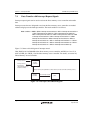
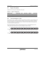
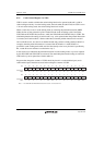
0
1
127
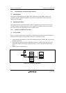
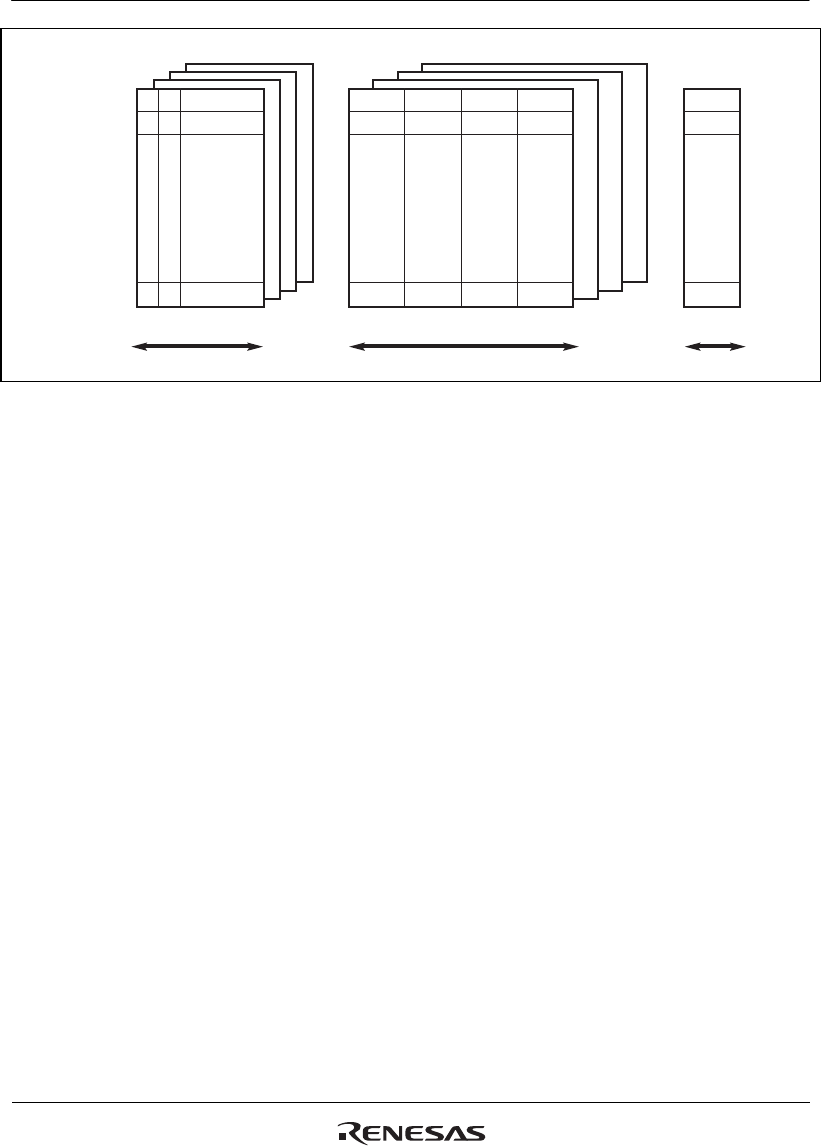
V U LW0 LW1 LW2
LW3
0
1
127
LRU
23 (1 + 1 + 21) bits
128 (32 × 4) bits
6 bits
LW0 to LW3: Longword data 0 to 3
Entry 0
Entry 1
Entry 127
Tag address
Address array (ways 0 to 3) Data array (ways 0 to 3)
.
.
.
.
.
.
.
.
.
.
.
.
.
.
.
.
.
.
Figure 8.1 Operand Cache Structure
(1) Address Array
The V bit indicates whether the entry data is valid. When the V bit is 1, data is valid; when 0, data
is not valid.
The U bit (only for operand cache) indicates whether the entry has been written to in write-back
mode. When the U bit is 1, the entry has been written to; when 0, it has not.
The tag address holds the physical address used in the access to external memory or large-capacity
on-chip RAM. It consists of 21 bits (address bits 31 to 11) used for comparison during cache
searches. In this LSI, the addresses of the cache-enabled space are H'00000000 to H'1FFFFFFF
(see section 9, Bus State Controller), and therefore the upper three bits of the tag address are
cleared to 0.
The V and U bits are initialized to 0 by a power-on reset but not initialized by a manual reset or in
software standby mode. The tag address is not initialized by a power-on reset or manual reset or in
software standby mode.
(2) Data Array
Holds a 16-byte instruction or data. Entries are registered in the cache in line units (16 bytes).
The data array is not initialized by a power-on reset or manual reset or in software standby mode.