


Section 9 Bus State Controller
Page 322 of 2108 R01UH0134EJ0400 Rev. 4.00
Sep 24, 2014
SH7262 Group, SH7264 Group
(7) Bank Active
The SDRAM bank function can be used to support high-speed access to the same row address.
When the BACTV bit in SDCR is 1, access is performed using commands without auto-precharge
(READ or WRIT). This function is called bank-active function. This function is valid only for area
3. When area 3 is set to bank-active mode, area 2 should be set to normal space or SRAM with
byte selection. When areas 2 and 3 are both set to SDRAM, auto precharge mode must be set.
When the bank-active function is used, precharging is not performed when the access ends. When
accessing the same row address in the same bank, it is possible to issue the READ or WRIT
command immediately, without issuing an ACTV command. As SDRAM is internally divided
into several banks, it is possible to activate one row address in each bank. If the next access is to a
different row address, a PRE command is first issued to precharge the relevant bank, then when
precharging is completed, the access is performed by issuing an ACTV command followed by a
READ or WRIT command. If this is followed by an access to a different row address, the access
time will be longer because of the precharging performed after the access request is issued. The
number of cycles between issuance of the PRE command and the ACTV command is determined
by the WTRP1 and WTPR0 bits in CS3WCR.
In a write, when an auto-precharge is performed, a command cannot be issued to the same bank
for a period of Trwl + Tap cycles after issuance of the WRITA command. When bank active mode
is used, READ or WRIT commands can be issued successively if the row address is the same. The
number of cycles can thus be reduced by Trwl + Tap cycles for each write.
There is a limit on tRAS, the time for placing each bank in the active state. If there is no guarantee
that there will not be a cache hit and another row address will be accessed within the period in
which this value is maintained by program execution, it is necessary to set auto-refresh and set the
refresh cycle to no more than the maximum value of tRAS.
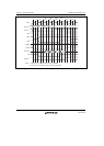
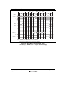
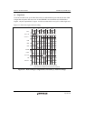
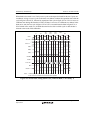
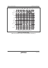
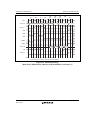
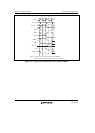
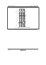
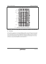
A burst read cycle without auto-precharge is shown in figure 9.20, a burst read cycle for the same
row address in figure 9.21, and a burst read cycle for different row addresses in figure 9.22.
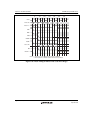
Similarly, a single write cycle without auto-precharge is shown in figure 9.23, a single write cycle
for the same row address in figure 9.24, and a single write cycle for different row addresses in
figure 9.25.
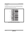
In figure 9.21, a Tnop cycle in which no operation is performed is inserted before the Tc cycle that
issues the READ command. The Tnop cycle is inserted to acquire two cycles of CAS latency for
the DQMx signal that specifies the read byte in the data read from the SDRAM. If the CAS
latency is specified as two cycles or more, the Tnop cycle is not inserted because the two cycles of
latency can be acquired even if the DQMx signal is asserted after the Tc cycle.