R01UH0134EJ0400 Rev. 4.00 Page 2075 of 2108
Sep 24, 2014
Item Page Revision (See Manual for Details)
16.4.5 Data Format
(5) LSB First Transfer (16-
Bit Data)
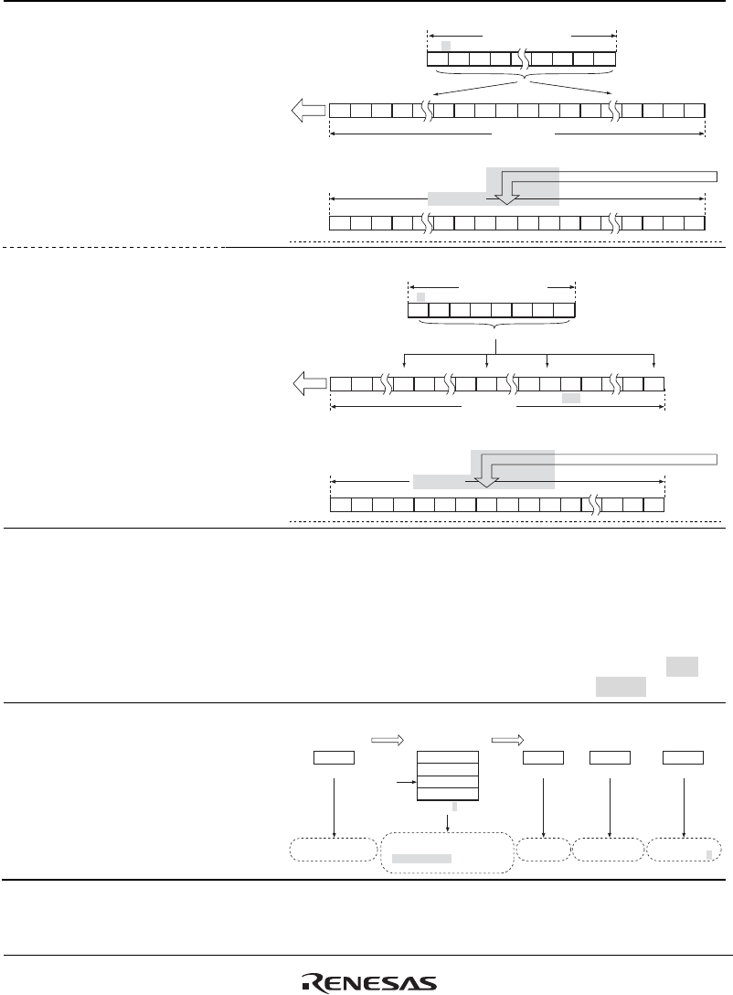
Figure 16.12 LSB First
Transfer (16-Bit Data)
824 Figure amended
Bit 15
Transfer start
Transfer end
Bit 0
0 tiB51 tiB13 tiB
T15 T14 T13 T12 T11 T03 T02 T01 T00
T00 T01 T02 T03 T04 T12 T13 T14 T15 T02 T03 T11 T12 T13 T14 T15T00 T01
Transmit buffer (SPTX)
Shift register
Output
Bit 31
Bit 16
Bit 0
R00 R01 R02 R03 R04 R12 R13 R14 R15 T02 T03 T11 T12 T13 T14 T15T00 T01
Shift register
Input
Copy
(6) LSB First Transfer (8-Bit
Data)
Figure 16.13 LSB First
Transfer (8-Bit Data)
826 Figure amended
Bit 7
Transfer start
Transfer end
Bit 0
0 tiB7 tiB13 tiB
T07 T06 T05 T04 T03 T02 T01 T00
T00 T01 T00 T07 T00 T05 T06 T07 T05 T00 T01 T11 T06 T07T06 T07
Transmit buffer (SPTX)
Shift register
Output
Bit 31 Bit 0
R00 R01 R02 R03 R04 R05 R06 R07 T00 T03 T04 T05 T06 T07T01 T02
Bit 24
Input
Copy
Shift register
16.4.7 Initialization 832 Description amended
If 0 is written to the SPE bit in the control register (SPCR)
or this module clears the SPE bit to 0 because of the
detection of a mode fault error, this module disables the
module function, and initializes a part of the module
function. When a power-on reset is generated, this module
initializes all of the module function. An explanation of
initialization by the clearing of the SPE bit follows.
16.4.8 SPI Operation
(1) Multi-Master Mode
Operation
(c) Sequence Control
Figure 16.15 Determination
Procedure of Serial Transfer
Mode in Master Mode
834 Figure amended
SSL negate delay
= 1 RSPCK
Next-access delay
= 3 RSPCK + 2 Bφ
SCKD, SSLND, and SPND must be
referenced. MSB first, 8 bits,
SSL not retained, base division
ratio = 1 CPOL = 0, CPHA = 0
Sequence determined
Pointer
SPCP1
and
SPCP
0
Determine transfer
format
Refer to SCKD, SSLND, and SPND (if necessary)
SPCMD0
SPCMD1
SPCMD2
SPCMD3
SPSCR
Sequence is formed in
SPCMD0 to SPCMD2
RSPCK delay
= 2 RSPCK
SCKD SSLND SPND
H' H20'01
H'E700
H'00 H'02


