Section 16 Renesas Serial Peripheral Interface
R01UH0134EJ0400 Rev. 4.00 Page 813 of 2108
Sep 24, 2014
SH7262 Group, SH7264 Group
16.4.4 Transfer Format
(1) CPHA = 0
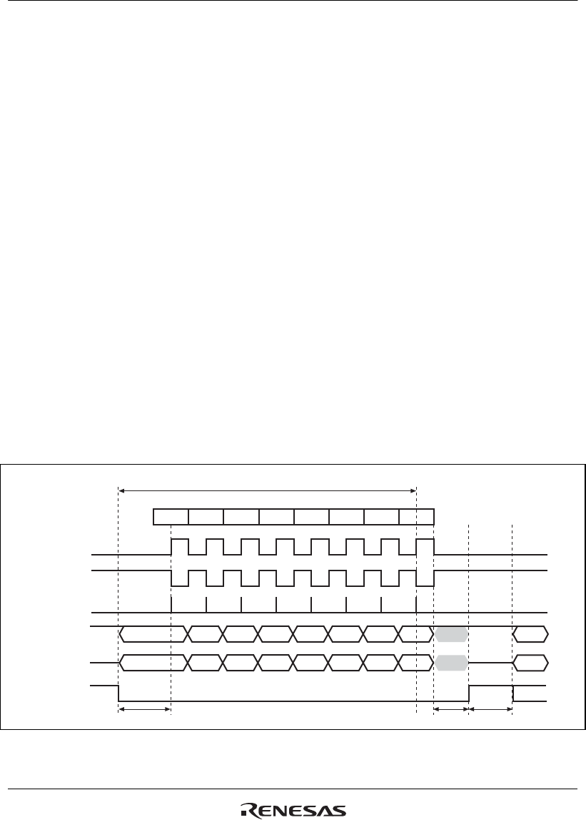
Figure 16.6 shows a sample transfer format for the serial transfer of 8-bit data when the CPHA bit
in the command register (SPCMD) is 0. In figure 16.6, RSPCK (CPOL = 0) indicates the RSPCK
signal waveform when the CPOL bit in SPCMD is 0; RSPCK (CPOL = 1) indicates the RSPCK
signal waveform when the CPOL bit is 1. The sampling timing represents the timing at which this
module fetches serial transfer data into the shift register. The input/output directions of the signals
depend on the settings of this module. For details, see section 16.4.2, Pin Control.
When the CPHA bit is 0, the driving of valid data to the MOSI and MISO signals commences at
an SSL signal assertion timing. The first RSPCK signal change timing that occurs after the SSL
signal assertion becomes the first transfer data fetching timing. After this timing, data is sampled
at every 1 RSPCK cycle. The change timing for MOSI and MISO signals is always 1/2 RSPCK
cycle after the transfer data fetch timing. The settings in the CPOL bit do not affect the RSPCK
signal operation timing; they only affect the signal polarity.
t1 denotes a period from an SSL signal assertion to RSPCK oscillation (RSPCK delay). t2 denotes
a period from the cessation of RSPCK oscillation to an SSL signal negation (SSL negation delay).
t3 denotes a period in which SSL signal assertion is suppressed for the next transfer after the end
of serial transfer (next-access delay). t1, t2, and t3 are controlled by a master device running on
the system. For a description of t1, t2, and t3 when this module is in master mode, see section
16.4.3 (1), Master/Slave (with This LSI Acting as Master).
Serial transfer period
12345678
RSPCK
cycle
Start
End
RSPCK
(CPOL = 0)
RSPCK
(CPOL = 1)
Sampling
timing
MOSI
MISO
SSL
t1 t2
t3
Figure 16.6 Transfer Format (CPHA = 0)


