Section 9 Bus State Controller
R01UH0134EJ0400 Rev. 4.00 Page 347 of 2108
Sep 24, 2014
SH7262 Group, SH7264 Group
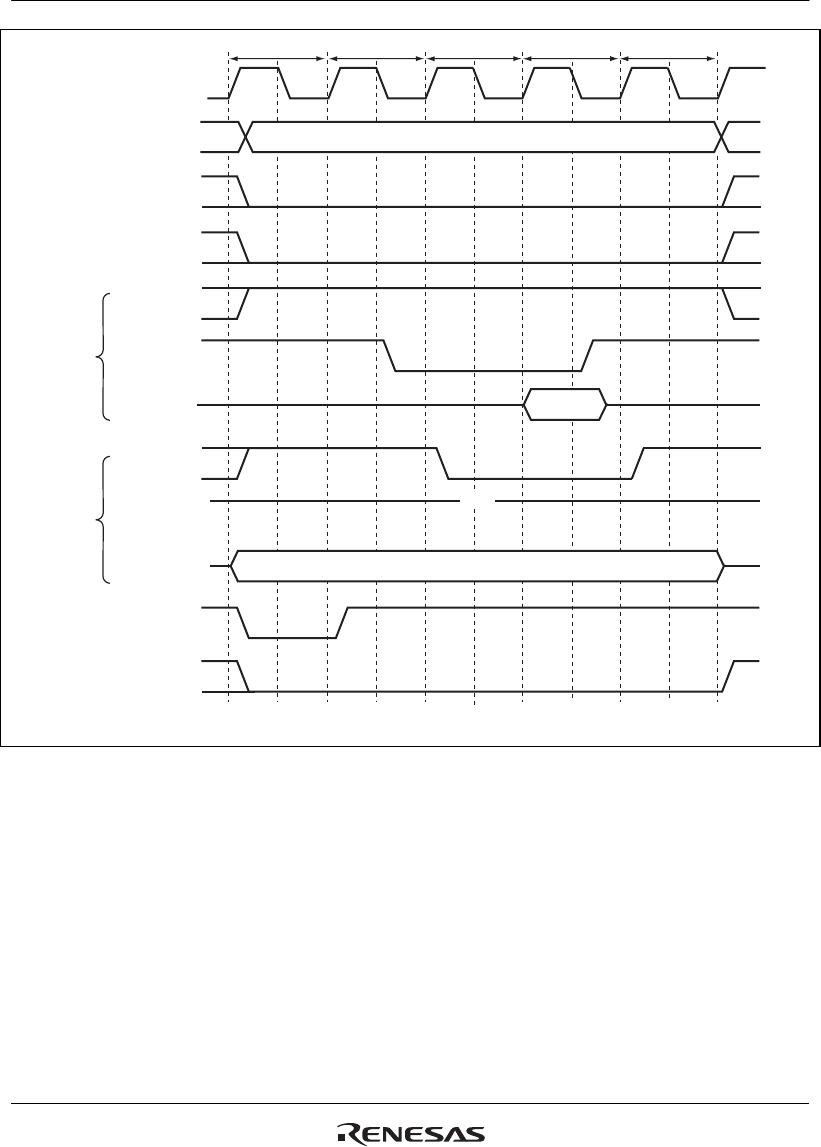
T2 TfTh T1 Tw
High
CKIO
A25 to A0
CSn
WEn
RD/WR
RD
RD
D15 to D0
D15 to D0
RD/WR
BS
DACKn*
Read
Write
Note: * The waveform for DACKn is when active low is specified.
Figure 9.36 Wait Timing for SRAM with Byte Selection (BAS = 1)
(SW[1:0] = 01, WR[3:0] = 0001, HW[1:0] = 01)


