Section 11 Multi-Function Timer Pulse Unit 2
Page 588 of 2108 R01UH0134EJ0400 Rev. 4.00
Sep 24, 2014
SH7262 Group, SH7264 Group
(2) Output Compare Output Timing
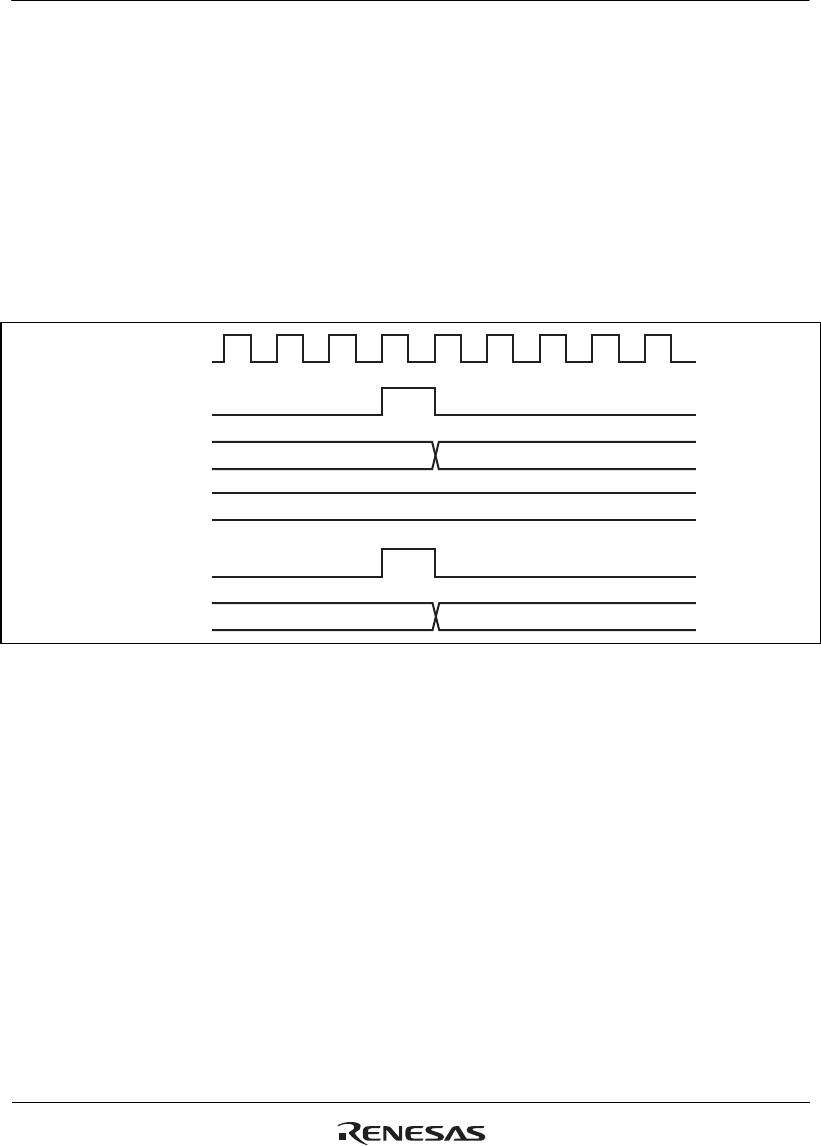
A compare match signal is generated in the final state in which TCNT and TGR match (the point
at which the count value matched by TCNT is updated). When a compare match signal is
generated, the output value set in TIOR is output at the output compare output pin (TIOC pin).
After a match between TCNT and TGR, the compare match signal is not generated until the
TCNT input clock is generated.
Figure 11.81 shows output compare output timing (normal mode and PWM mode) and Figure
11.82 shows output compare output timing (complementary PWM mode and reset synchronous
PWM mode).
TGR
TCNT
TCNT input
clock
N
N
N + 1
Compare
match signal
TIOC pin
Pφ
Figure 11.81 Output Compare Output Timing (Normal Mode/PWM Mode)


