Section 10 Direct Memory Access Controller
Page 428 of 2108 R01UH0134EJ0400 Rev. 4.00
Sep 24, 2014
SH7262 Group, SH7264 Group
CKIO
DREQ
(Overrun 0 at
high level)
DACK
(Active-high)
Bus cycle
2nd
acceptance
CPU CPU DMA
CKIO
DREQ
(Overrun 1 at
high level)
DACK
(Active-high)
Bus cycle
1st acceptance
2nd acceptance
Non sensitive period
Non sensitive period
CPU CPU DMA
3rd
acceptance
DMA
Acceptance
start
Acceptance
start
Acceptance
start
1st acceptance
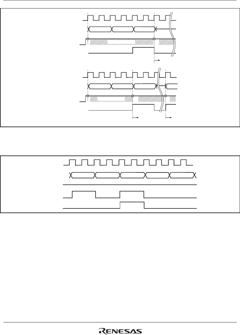
Figure 10.14 Example of DREQ Input Detection in Burst Mode Level Detection
Figure 10.15 shows the TEND output timing.
CKIO
DACK
DREQ
TEND
Bus cycle
End of DMA transfer
DMA
CPU CPU
CPU
DMA
Figure 10.15 Example of DMA Transfer End Signal Timing
(Cycle Steal Mode Level Detection)
The unit of the DMA transfer is divided into multiple bus cycles when 16-byte transfer is
performed for an 8-bit or16-bit external device or when word transfer is performed for an 8-bit
external device. When a setting is made so that the DMA transfer size is divided into multiple bus
cycles and the CS signal is negated between bus cycles, note that DACK and TEND are divided
like the CS signal for data alignment as shown in figure 10.16. Figures 10.11 to 10.15 show the
cases where DACK and TEND are not divided in the DMA transfer.


