Section 10 Direct Memory Access Controller
R01UH0134EJ0400 Rev. 4.00 Page 373 of 2108
Sep 24, 2014
SH7262 Group, SH7264 Group
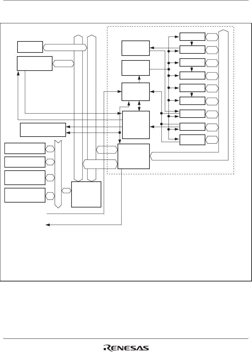
Figure 10.1 shows the block diagram of this module.
On-chip
peripheral module
DMA transfer request signal
DMA transfer acknowledge signal
Peripheral bus
Internal bus
External ROM
On-chip
memory
Interrupt controller
DREQ0, DREQ1*
HEIn
DACK0, DACK1*,
TEND0, TEND1*
External RAM
Bus
interface
Bus state
controller
External device
(memory mapped)
External device
(with acknowledge)
Request
priority
control
Start-up
control
Register
control
Iteration
control
RDMATCR_n
DMATCR_n
RSAR_n
SAR_n
DAR_n
RDAR_n
CHCR_n
DMAOR
DMARS0
to DMARS7
RDMATCR:
DMATCR:
RSAR:
SAR:
RDAR:
DAR:
DMA reload transfer count register
DMA transfer count register
DMA reload source address register
DMA source address register
DMA reload destination address register
DMA destination address register
CHCR:
DMAOR:
DMARS0 to DMARS7:
HEIn:
DEIn:
n = 0 to 15
DMA channel control register
DMA operation register
DMA extension resource selectors 0 to 7
DMA transfer half-end interrupt request to the CPU
DMA transfer end interrupt request to the CPU
DEIn
[Legend]
Note: * Pins in channel 1 can be used only in the SH7264 Group.
Figure 10.1 Block Diagram


