Section 10 Direct Memory Access Controller
R01UH0134EJ0400 Rev. 4.00 Page 419 of 2108
Sep 24, 2014
SH7262 Group, SH7264 Group
Auto request, external request, and on-chip peripheral module request are available for the transfer
request. DACK can be output in read cycle or write cycle in dual address mode. The AM bit in the
channel control register (CHCR) can specify whether the DACK is output in read cycle or write
cycle.
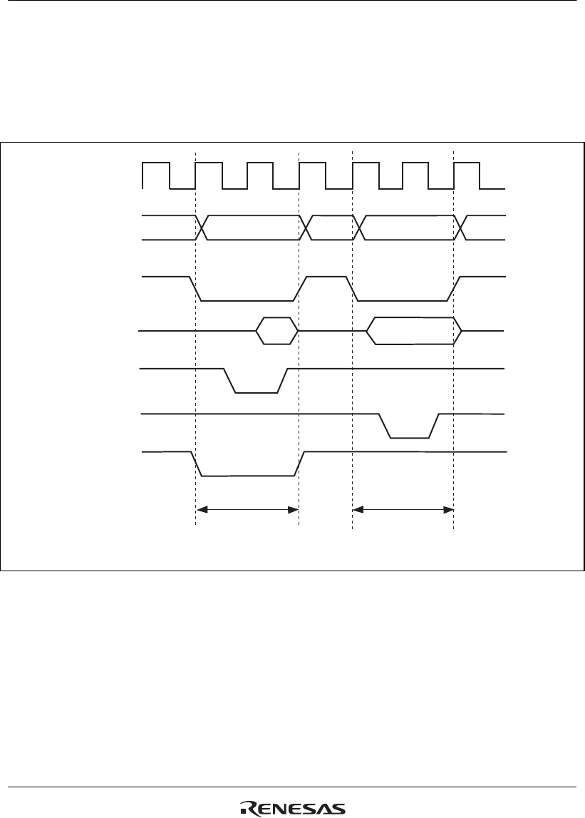
Figure 10.4 shows an example of DMA transfer timing in dual address mode.
CKIO
A25 to A0
D15 to D0
DACKn
(Active-low)
CSn
WEn
RD
Data read cycle
Data write cycle
(1st cycle)
(2nd cycle)
Transfer source
address
Transfer destination
address
Note: In transfer between external memories, with DACK output in the read cycle,
DACK output timing is the same as that of CSn.
Figure 10.4 Example of DMA Transfer Timing in Dual Mode
(Transfer Source: Normal Memory, Transfer Destination: Normal Memory)


