Section 11 Multi-Function Timer Pulse Unit 2
R01UH0134EJ0400 Rev. 4.00 Page 577 of 2108
Sep 24, 2014
SH7262 Group, SH7264 Group
00011223 3
0011223 3
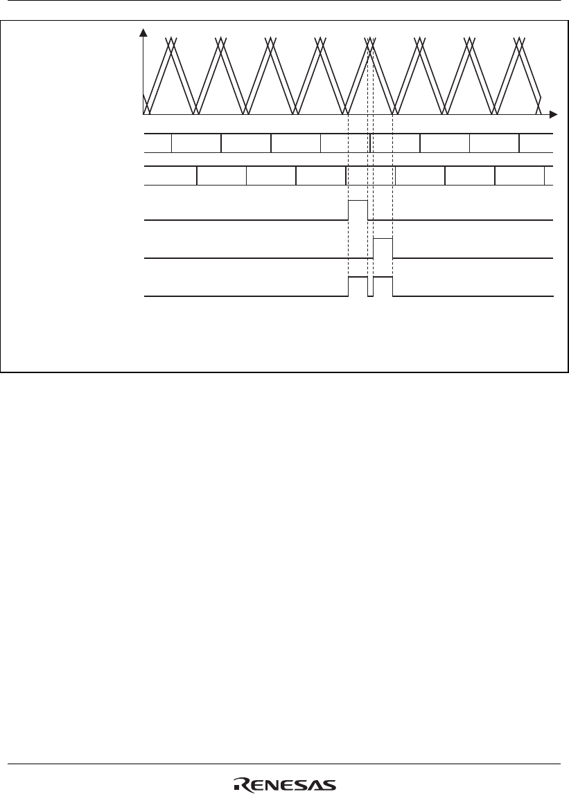
Skipping counter 3ACNT
Skipping counter 4VCNT
Buffer transfer-enabled period
(T3AEN is set to 1)
Buffer transfer-enabled period
(T4VEN is set to 1)
Buffer transfer-enabled period
(T3AEN and T4VEN are set to 1)
Note: * The MD bits 3 to 0 = 1111 in TMDR_3, buffer transfer at the crest and the
trough is selected.
The skipping count is set to three.
T3AEN and T4VEN are set to 1.
Figure 11.72 Relationship between Bits T3AEN and T4VEN in TITCR and Buffer
Transfer-Enabled Period
(4) Complementary PWM Mode Output Protection Function
Complementary PWM mode output has the following protection function.
(a) Register and counter miswrite prevention function
With the exception of the buffer registers, which can be rewritten at any time, access by the CPU
can be enabled or disabled for the mode registers, control registers, compare registers, and
counters used in complementary PWM mode by means of the RWE bit in the timer read/write
enable register (TRWER). The applicable registers are some (21 in total) of the registers in
channels 3 and 4 shown in the following:
TCR_3 and TCR_4, TMDR_3 and TMDR_4, TIORH_3 and TIORH_4, TIORL_3 and
TIORL_4, TIER_3 and TIER_4, TCNT_3 and TCNT_4, TGRA_3 and TGRA_4, TGRB_3
and TGRB_4, TOER, TOCR, TGCR, TCDR, and TDDR.
This function enables miswriting due to CPU runaway to be prevented by disabling CPU access to
the mode registers, control registers, and counters. When the applicable registers are read in the
access-disabled state, undefined values are returned. Writing to these registers is ignored.


