Section 17 I
2
C Bus Interface 3
R01UH0134EJ0400 Rev. 4.00 Page 851 of 2108
Sep 24, 2014
SH7262 Group, SH7264 Group
17.2 Input/Output Pins
Table 17.1 shows the pin configuration.
Table 17.1 Pin Configuration
Pin Name Symbol I/O Function
Serial clock SCL0 to SCL2 I/O I
2
C serial clock input/output
Serial data SDA0 to SDA2 I/O I
2
C serial data input/output
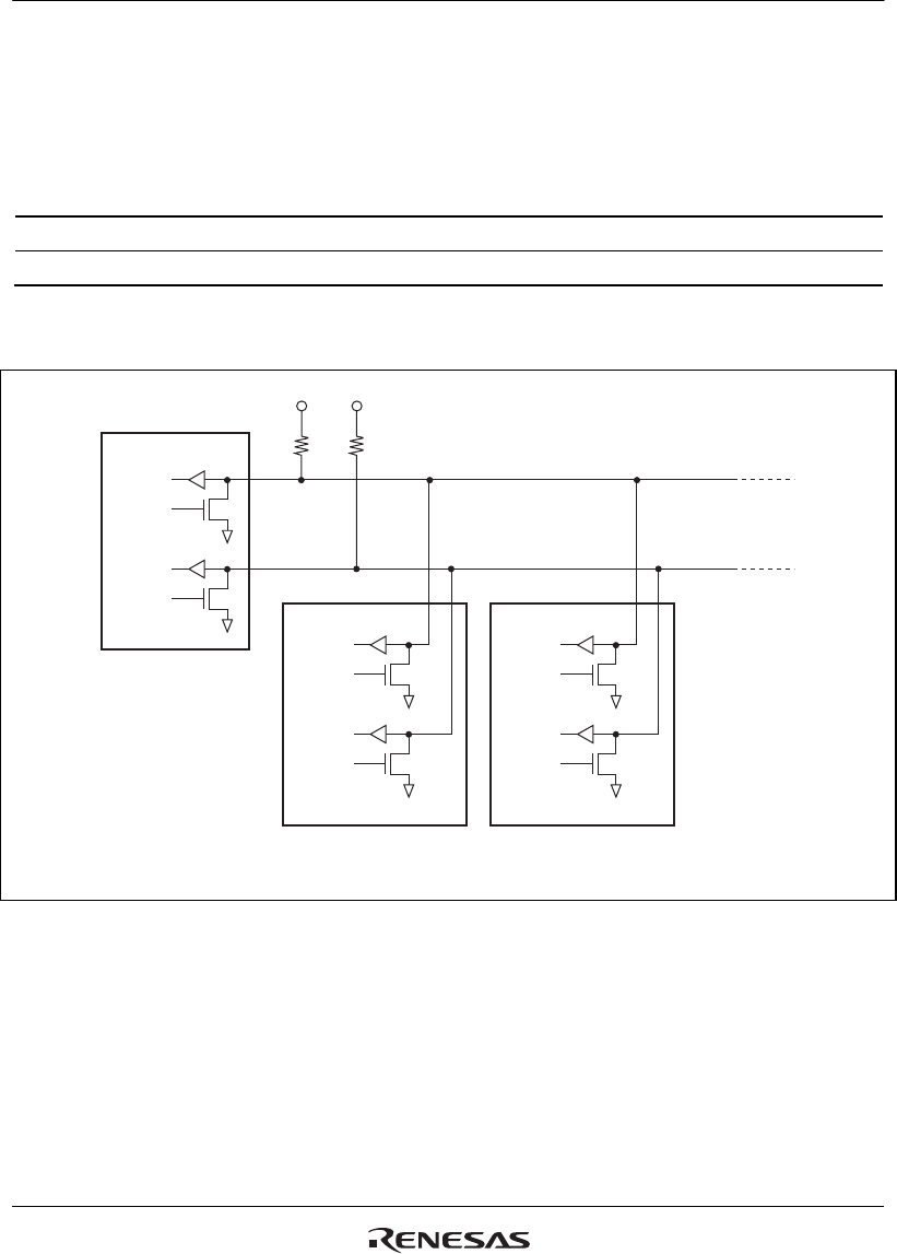
Figure 17.2 shows an example of I/O pin connections to external circuits.
PVcc* PVcc*
SCL in
SCL out
SCL
SDA in
SDA out
SDA
SCL
SDA
SCL in
SCL out
SCL
SDA in
SDA out
SDA
SCL in
SCL out
SCL
SDA in
SDA out
SDA
Note: * Turn on/off PVcc for the I
2
C bus power supply and for this LSI simultaneously.
(Master)
(Slave 1) (Slave 2)
Figure 17.2 External Circuit Connections of I/O Pins


