


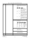
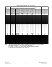
RFL NCM RFL Electronics Inc.
November 6, 2007 22 (973) 334-3100
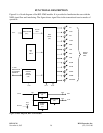
NCM BACKPLANE AND POWER CONNECTIONS
The NCM occupies a single slot in the multiplexer chassis and conforms to the RFL IMUX 2000 back
plane signal format. All T1 and E1 signals, and control signals passing through the back plane,
interface with the cross point Lattice device (U6). All inputs and outputs of the Lattice Device are
pulled up to 3.3V through approximately 50K Ohms.
The NCM requires digital +5Vdc and digital ground connections to the back plane. TP2 and TP12 are
the ground test points. The digital +5V from the back plane is routed to the Hot Swap Controller (U1,
which controls the ramp of the power to all of the ICs. The ramped digital +5V supply is only directly
used to provide power to the LEDs, DS1 through DS13, and can be monitored at TP1.
Linear voltage regulators U3 and U4 step-down the +5V digital supply to produce +2.5V and +3.3V
supplies respectively. The +2.5V is used exclusively to power the Actel FPGA (U2). The 3.3V is used
to power the Lattice device (U6), the I/O of the Actel (U2), the 49.152mHz oscillator (U11), and the
pull-up resistors on the module. The +2.5V and 3.3V supplies can be monitored at TP3 and TP4
respectively. All pins which connect to the back plane, except for voltages and grounds, are cut back to
prevent components from being driven before the module is fully powered.
TX INPUT PORTS
The NCM module supports one or two TX input ports depending on the interface adapter installed (i.e.
MA-402I, MA-485, or MA-490). An asynchronous data signal is applied to a TX input of the
appropriate interface adapter. The data signal is converted from RS-232, MA-485, or Ethernet to a
logic signal on the interface adapter before being fed through the back plane to the NCM module.
These logic signals pass through the Lattice device (U6), and are applied to the Actel’s (U2) UART
receive section. Indication of TX input activity can be observed at the IN1 and IN2 LEDs, and via the
NMS software.
RX OUTPUT PORTS
The asynchronous logic data signal is transmitted by the UART Transmit section of the Actel (U2),
and passes through the Lattice device and back plane to the interface adapter. The interface adapter
converts the logic signal to the appropriate interface format (i.e. RS-232, RS-485, or Ethernet),
depending on the interface adapter installed. The CTS and RLSD are always active for RS-232
applications (MA-402I) that require these to be active. Indication of RX output activity can be
observed at OUT1 and OUT2, and via the NMS software.
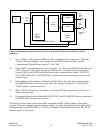
LOGIC ARRAY (ACTEL DESIGN)
The Actel FPGA controls, processes, and coordinates all functions of the NCM. It interfaces switches,
LEDs, SCB bus signals, T1/E1 bus signals, and I/O control lines. The Actel design can be broken
down into the following nine functions: SCB, Application Modes and Interfaces, UART Receive,
UART Transmit, T1 Transmit, T1 Receive, Rogue Control, Loop-backs, and Baud and Clock
Generator.