


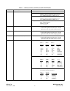
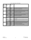
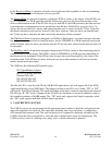
FUNCTIONAL DESCRIPTION
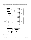
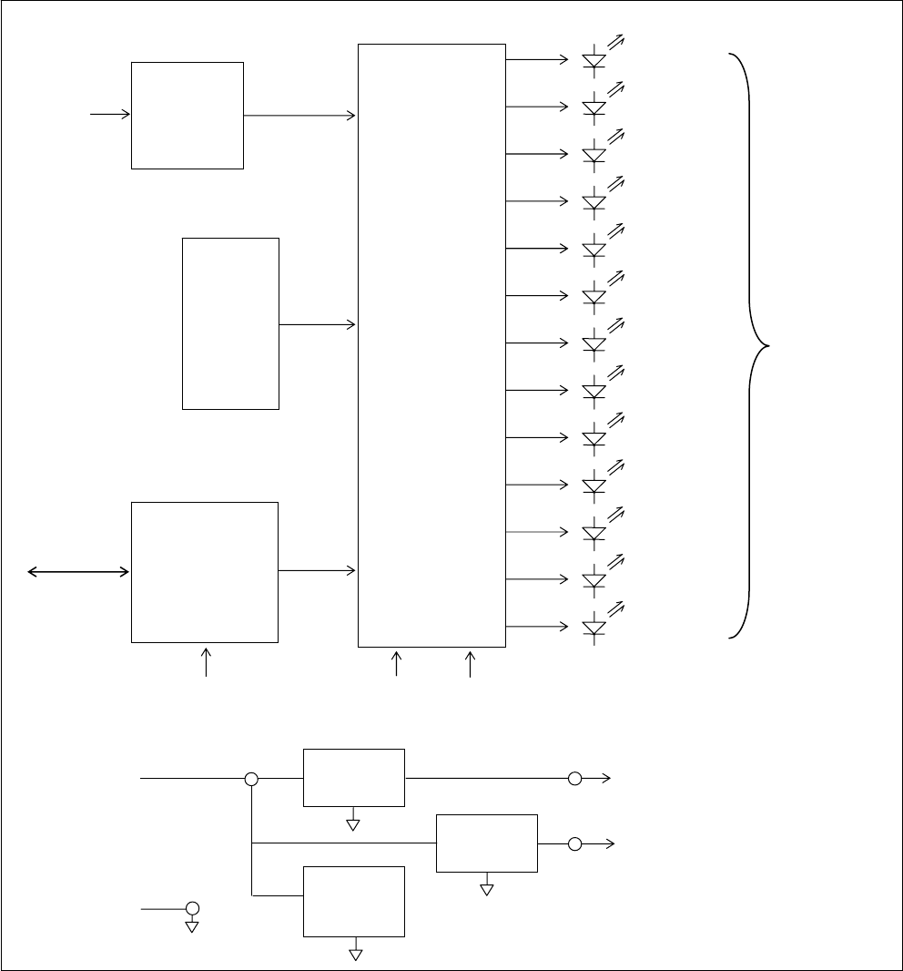
Figure 8 is a block diagram of the RFL NMS module. It is provided to familiarize the user with the
NMS signal flow and interfacing. The figure shows signal flow in the transmit and receive modes of
operation.
SW1
to
SW10
OSCILLATOR
(U11)
Actel
FPGA
(U2)
CROSS
POINT
LATTICE
(U6)
3.3 V
T1 & E1
BACKPLANE
& CONTROL
SIGNALS
3.3V 3.3 V 2.5V
IN1
OUT1
IN2
OUT2
RXB
TXA
RXA
TXB
EQLB
PALB
ADRA
ADRB
SERVICE
49.152
mHz
REGULATOR
(U3)
REGULATOR
(
U4
)
POWER
RESET
(U1)
TP1
TP3
2.5V
TP4
3.3V
TP2,
TP12
+5Vdc
Ground
FRONT
PANEL
LEDs
Figure 8. Block diagram, RFL NCM module.
RFL NCM RFL Electronics Inc.
November 6, 2007 20 (973) 334-3100