Section 25 NAND Flash Memory Controller
Page 1290 of 2108 R01UH0134EJ0400 Rev. 4.00
Sep 24, 2014
SH7262 Group, SH7264 Group
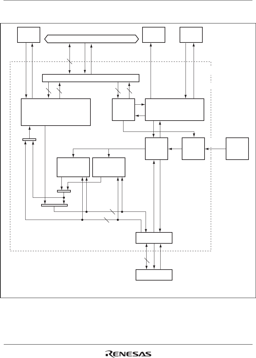
Figure 25.1 shows a block diagram.
Peripheral bus
Interrupt requests
(4 lines)
Control signal
DMA transfer
requests (2 lines)
Direct
memory
access
controller
Peripheral bus interface
32
32
Registers
State
machine
Transmit/
receive
control
3-symbol
ECC
Flash memory
interface
NAND
Flash memory
FIFO
256 bytes
Interrupt
controller
Bus state
controller
32
8
8
8
32 32
4-symbol
ECC
Clock
pulse
generator
×1/2
×1/4
FCLK
QTSEL
Bus mastership
request
acknowledge
NAND
flash memory
controller
Bus mastership
request
Note: FCLK is the operating clock for flash memory interface signals.
The division ratio is specified by register FLCMNCR.
Peripheral
clock
Figure 25.1 Block Diagram


