Section 9 Bus State Controller
Page 326 of 2108 R01UH0134EJ0400 Rev. 4.00
Sep 24, 2014
SH7262 Group, SH7264 Group
Tr Tc1
CKIO
A25 to A0
CS3
RD/WR
RAS
DQMx
D15 to D0
BS
DACKn*
2
A12/A11*
1
CAS
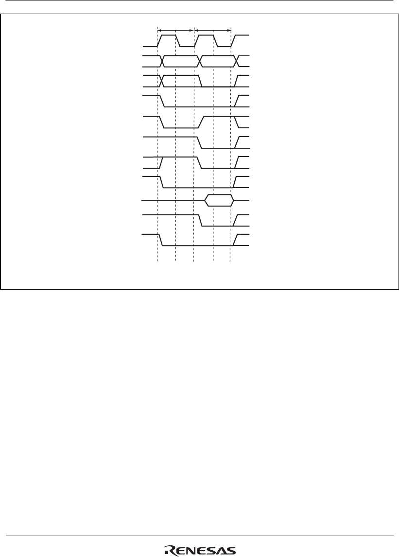
Notes: 1. Address pin to be connected to pin A10 of SDRAM.
2. The waveform for DACKn is when active low is specified.
Figure 9.23 Single Write Timing (Bank Active, Different Bank)


