Section 7 Interrupt Controller
Page 162 of 2108 R01UH0134EJ0400 Rev. 4.00
Sep 24, 2014
SH7262 Group, SH7264 Group
7.3.1 Interrupt Priority Registers 01, 02, 05 to 22 (IPR01, IPR02, IPR05 to IPR22)
IPR01, IPR02, and IPR05 to IPR22 are 16-bit readable/writable registers in which priority levels
from 0 to 15 are set for IRQ interrupts, PINT interrupts, and on-chip peripheral module interrupts.
Table 7.3 shows the correspondence between the interrupt request sources and the bits in IPR01,
IPR02, and IPR05 to IPR22.
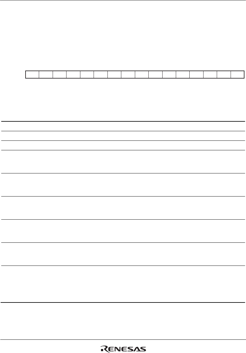
15 14 13 12 11 10 9 8 7 6 5 4 3 2 1 0
0000000000000000
R/W R/W R/W R/W R/W R/W R/W R/W R/W R/W R/W R/W R/W R/W R/W R/W
Bit:
Initial value:
R/W:
Table 7.3 Interrupt Request Sources and IPR01, IPR02, and IPR05 to IPR22
Register Name Bits 15 to 12 Bits 11 to 8 Bits 7 to 4 Bits 3 to 0
IPR01 IRQ0 IRQ1 IRQ2 IRQ3
IPR02 IRQ4 IRQ5 IRQ6 IRQ7
IPR05 PINT7 to PINT0 Reserved Reserved Reserved
IPR06 Direct memory
access controller
channel 0
Direct memory
access controller
channel 1
Direct memory
access controller
channel 2
Direct memory
access controller
channel 3
IPR07 Direct memory
access controller
channel 4
Direct memory
access controller
channel 5
Direct memory
access controller
channel 6
Direct memory
access controller
channel 7
IPR08 Direct memory
access controller
channel 8
Direct memory
access controller
channel 9
Direct memory
access controller
channel 10
Direct memory
access controller
channel 11
IPR09 Direct memory
access controller
channel 12
Direct memory
access controller
channel 13
Direct memory
access controller
channel 14
Direct memory
access controller
channel 15
IPR10 USB 2.0
host/function
module
Video display
controller 3
Compare match
timer channel 0
Compare match
timer channel 1
IPR11 Bus state
controller
Watchdog timer Multi-function
timer pulse unit 2
channel 0
(TGI0A to TGI0D)
Multi-function
timer pulse unit 2
channel 0
(TCI0V, TGI0E,
TGI0F)


