Section 22 Renesas SPDIF Interface
Page 1186 of 2108 R01UH0134EJ0400 Rev. 4.00
Sep 24, 2014
SH7262 Group, SH7264 Group
Notes: 1. Channel status data requests do not support DMA.
2. When receiver user buffer overrun occurs, the current data in the buffer data of SPDIF
is overwritten by the next incoming data from SPDIF interface.
22.9.2 Receiver Module Initialization
The device defaults to an idle state when it comes out of reset, or can be put into an idle state by
writing 0 to bit RME in the CTRL register. Whilst idle the module has the following settings:
The receiver idle status bit is set to 1, all other status bits are cleared to 0.
Synchronization between channels 1 and 2 is set to 0 (0 for channel 1, 1 for channel 2).
Both Word_count and frame_count are set to 0.
Channel status registers, user data registers and audio data registers will retain its value prior to
putting the module into idle. To exit the idle state the user must write 1 to the bit RME in the
CTRL register.
22.9.3 Receiver Module Data Transfer
Once the module has left the idle state it is ready for data transfer. Data transfer timing can be
achieved in three ways. The transfer can be done by interrupts, or by polling the status register, or
by DMA. There is a shared interrupt line (transmit and receive) and a single receiver DMA request
line. Data transfer for the receiver can be interrupted by error signals caused by:
1. Clock recovery failure.
2. Transmission loss or interference – indicated by a preamble error.
3. Parity check failure.
Transmission loss or interference can cause the start of subframe or start of block preamble to be
misplaced or not present.
Parity check failure occurs when the parity bit is incorrect, this can be caused by any of the above.
Clock Recovery Deviation
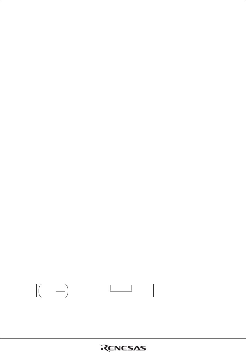
The receive margin for clock recovery is based on the following equation:
M = 0.5 − − (L − 0.5) F − (1 + F) × 100%
1
2N
D − 0.5
N


