


Intel® Solid-State Drive DC P3700 Series
Product Specification May 2015
22 330566-009US
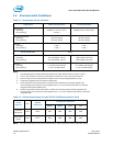
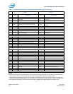
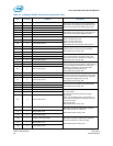
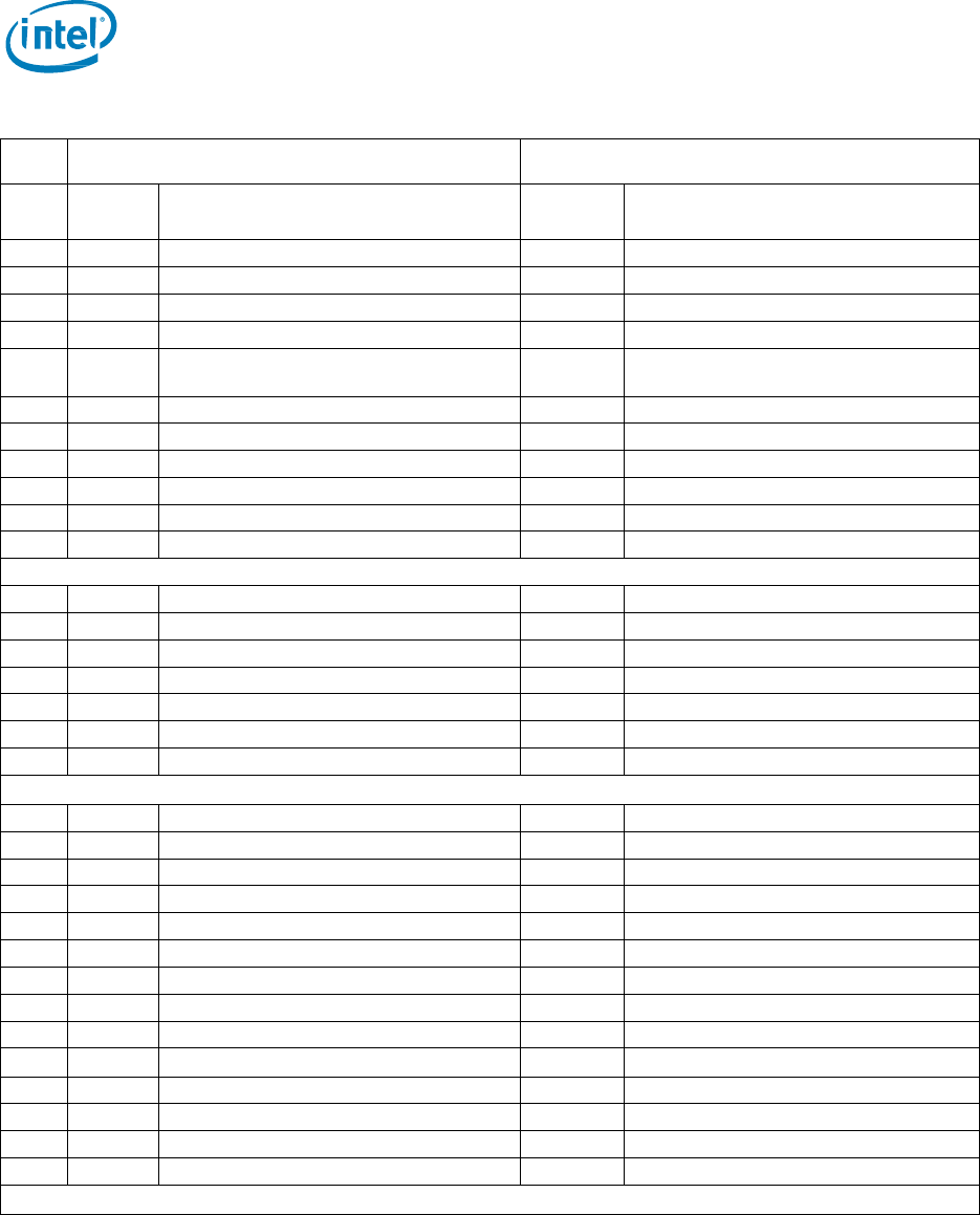
Table 17: Pin Definition for Add-In Card (Half Height Half Length) Form Factor
Side B
Side A
Pin
Name
Description
Name
Description
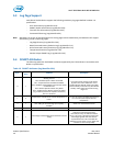
1
+12V
12V power
PRSNT1#
Hot-Plug presence detect
2
+12V
12V power
+12V
12V power
3
+12V
12V power
+12V
12V power
4
GND
Ground
GND
Ground
5
SMCLK
SMBus(System Management Bus) clock
JTAG2
TCK (Test Clock), clock input for JTAG
interface
6
SMDAT
SMBus (System Management Bus) data
JTAG3
TDI (Test Data Input)
7
GND
Ground / UART_HOST
JTAG4
TDO (Test Data Output)
8
+3.3V
3.3V power
JTAG5
TMS (Test Mode Select)
9
JTAG1
TRST# (Test Reset) resets the JTAG interface
+3.3V
3.3V power
10
3.3Vaux
3.3V auxiliary power
+3.3V
3.3V power
11
WAKE#
Signal for Link reactivation
PERST#
Fundamental reset
Mechanical Key
12
RSVD
Reserved
GND
Ground
13
GND
Ground
REFCLK+
Reference clock (differential pair)
14
PETp0
Transmitter differential pair, Lane 0
REFCLK-
Reference clock (differential pair)
15
PETn0
Transmitter differential pair, Lane 0
GND
Ground
16
GND
Ground
PERp0
Receiver differential pair, Lane 0
17
PRSNT2#
Hot-Plug presence detect
PERn0
Receiver differential pair, Lane 0
18
GND
Ground
GND
Ground
End of the x1 Connector
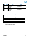
19
PETp1
Transmitter differential pair, Lane 1
RSVD
Reserved
20
PETn1
Transmitter differential pair, Lane 1
GND
Ground
21
GND
Ground
PERp1
Receiver differential pair, Lane 1
22
GND
Ground
PERn1
Receiver differential pair, Lane 1
23
PETp2
Transmitter differential pair, Lane 2
GND
Ground
24
PETn2
Transmitter differential pair, Lane 2
GND
Ground
25
GND
Ground
PERp2
Receiver differential pair, Lane 2
26
GND
Ground
PERn2
Receiver differential pair, Lane 2
27
PETp3
Transmitter differential pair, Lane 3
GND
Ground
28
PETn3
Transmitter differential pair, Lane 3
GND
Ground
29
GND
Ground
PERp3
Receiver differential pair, Lane 3
30
RSVD
Reserved
PERn3
Receiver differential pair, Lane 3
31
PRSNT2#
Hot-Plug presence detect
GND
Ground
32
GND
Ground
RSVD
Reserved
End of the x4 Connector
NOTES:
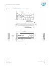
All pins are numbered in ascending order from the left to the right, with side A on the top of the centerline and
side B on the bottom of the centerline, use the reference drawing in Fig2, with the logo visible.
The PCI Express interface pins PETpx, PETnx, PERpx, and PERnx are named with the following convention: “PE”
stands for PCI Express high speed, “T” for Transmitter, “R” for Receiver, “p” for positive (+) and “n” for negative (-).
The sequential mating for Hot-Plug is accomplished by staggering the edge fingers on the add-in card.
§