


- 33 -
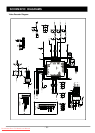
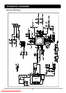
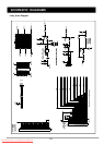
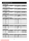
INFORMATION OF ICS
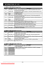
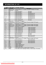
IC GM5221 PQFP-208 (DVI Input Port)
Pin No. Pin Name Description
126 VDD_RX0_1.8 VDD (1.8V) for TMDS input pair 2. Must be bypassed with external
capacitor to GND_RX0
127 AGND_RX0 Analog GND for TMDS input pair 0. Must be connected directly to the
analog ground plane.
128 RX0+ TMDS input pair 0
129 RX0- TMDS input pair 0
130 AVDD_RX0_3.3 Analog VDD (3.3V) for TMDS input pair 2. Must be bypassed with
capacitor to AGND_RX0
131 AGND_RXC Analog GND for TMDS input clock pair. Must be connected directly to
the analog ground plane.
132 RXC+ TMDS input clock pair
133 RXC- TMDS input clock pair
134 AVDD_RXC_3.3 Analog VDD (3.3V) for TMDS input clock pair.
Must be bypassed with 100pF capacitor to AGND_RXC.
136 GND_RXPLL Analog GND for the TMDS receiver internal PLL.
Must be connected directly to the analog ground plane.
137 VDD_RXPLL_1.8Analog VDD (1.8V) for the TMDS receiver internal PLL.
Must be bypassed with a capacitor to AGND_RXPLL.
138 CLK_OUT Reserved, unconnected.
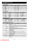
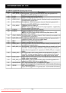
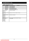
IC GM5221 PQFP-208 (RCLK PLL Pins)
Pin No. Pin Name Description
165 GND_RPLL Digital GND for ADC clocking circuit. Must be directly connected to the
digital system ground plane.
166 VDD_RPLL_1.8 Digital power (1.8V) for ADC digital logic. Must be bypassed with
capacitor to GND1_ADC.
168 AGND_RPLL Analog ground for the Reference DDS PLL. Must be directly connected
to the analog system ground plane.
169 XTAL Crystal oscillator output.
170 TCLK Reference clock (TCLK) from the 14.3MHz crystal oscillator.
171 AVDD_RPLL_3.3 Analog VDD (3.3V)
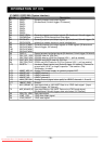
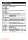
IC GM5221 PQFP-208 (Input Video Port)
Pin No. Pin Name Description
112 VCLK Video port data clock input. Up to 75Mhz
[Input, 5V-tolerant]
111 GPIO23/VDATA0 Input YUV data in 8-bit BT656 or GPIO23:16 if VPORT is disabled.
110 GPIO22/VDATA1 [Bi-Directional, 5V-tolerant]
109 GPIO21/VDATA2
108 GPIO20/VDATA3
107 GPIO19/VDATA4
106 GPIO18/VDATA5
103 GPIO17/VDATA6
102 GPIO16/VDATA7
Downloaded From TV-Manual.com Manuals