


- 41 -
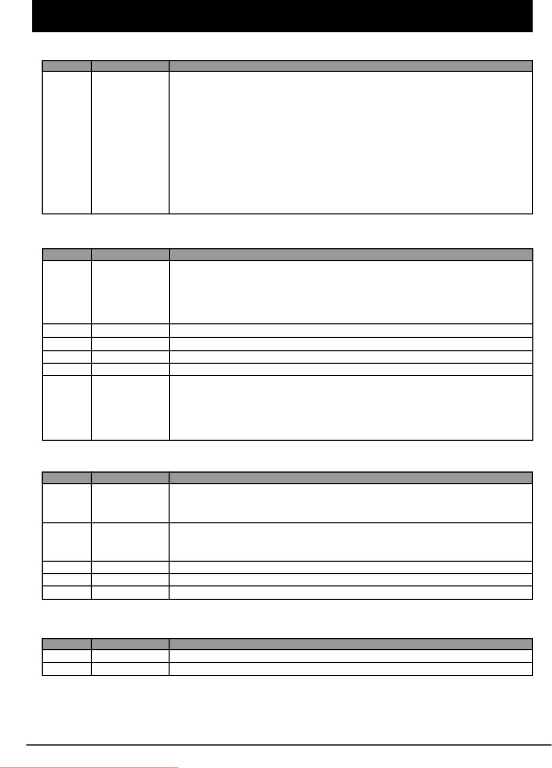
INFORMATION OF ICS
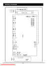
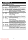
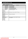
IC TVP5146PFP S-PQFP-G80 (Analog Video)
Pin No. Pin Name Description
80 VI_1_A
1 VI_1_B VI_1_x: Analog video input for CVBS/Pb/B/C
2 VI_1_C VI_2_x: Analog video input for CVBS/Y/G
7 VI_2_A VI_3_x: Analog video input for CVBS/Pr/R/C
8 VI_2_B VI_4_x: Analog video input for CVBS/Y
9 VI_2_C Up to 10 composite, 4 S-video, and 2 composite or 3 component
16 VI_3_A video input(or a combination thereof) can be supported.
17 VI_3_B The inputs must be ac-coupled. The recommended coupling
18 VI_3_C capacitor is 0.1μF.
23 VI_4_A The possible input configurations are listed in the input select
register at I
2
C subaddress 00h
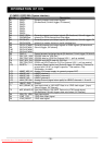
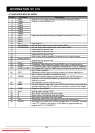
IC TVP5146PFP S-PQFP-G80 (Digital Video)
Pin No. Pin Name Description
57,58 C[9:0]/ Digital video output of CbCr, C[9] is MSB and C[0] is LSB. Unused
59,60, GPIO[9:0] outputs can be left unconnected. Also, these terminals can be
63,64, programmable general-purpose I/O.
65,66, For the 8-bit mode, the two LSBs are ignored.
69,70
58 D_BLUE Digital BLUE input from overlay device.
59 D_GREEN Digital GREEN input from overlay device.
60 D_RED Digital RED input from overlay device.
57 FSO Fast-switch overlay between digital RGB and any video.
43,44 Y[9:0] Digital video output of Y/YCbCr, Y[9] is MSB and Y[0] is LSB.
45,46, For the 8-bit mode, the two LSBs are ignored. Unused outputs
47,50, can be left unconnected.
51,52,
53,54
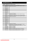
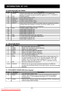
IC TVP5146PFP S-PQFP-G80 (Miscellaneous Signals)
Pin No. Pin Name Description
35 FSS/GPIO Fast-switch(blanking) input. Switching signal between the synchronous
component video(YPbPr/RGB) and the composite video input.
Programmable general-purpose I/O
37 GLCO/I2CA Genlock control output(GLCO). Two Genlock data formats are available:
TI format and real time control(RTC) format.
During reset, this terminal is an input used to program the I
2
C address LSB.
30 INTREQ Interrupt request
33 PWDN Power down input: 1=Power down 0=Normal mode
34 RESETB Reset input, active low
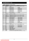
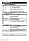
IC TVP5146PFP S-PQFP-G80 (Host Interface)
Pin No. Pin Name Description
28 SCL I
2
C clock input
29 SDA I
2
C data bus
Downloaded From TV-Manual.com Manuals